Successful designs are soon forgotten but failures are remembered
for years. Steering clear of these twelve don'ts will improve the
robustness of your designs.
It dawned on me recently that many flexible circuit designs are successful because of what designers don’t do in their designs rather than what they do include in their designs.
In the life of a flex circuit designer, many successful designs are soon forgotten as the next challenge crosses their desk. Failures, on the other hand, will stick in a designer’s mind for years. Good designers will learn from these less than perfect projects, and make sure that they never make that mistake again. In this article, I will share some of the things I’ve learned over 25 years of circuit design not to do to help ensure a reliable and cost effective design.
Documentation and Specifications
Don’t over-specify non-critical features on the drawing. Many circuit designs require the designer to generate a drawing package. While it is important to completely specify critical features, an over-specified drawing will not add robustness to the design, but will add additional cost.
A good drawing will have a flat view of the circuit with critical dimensions only. Remember that the electronic data (Gerber, DXF, ODB++) will define every feature of the circuit. Before a manufacturer can begin the set-up, every dimension on the drawing will have to be compared to the electronic data. If there are discrepancies (which routinely happen), they must be worked out between the manufacturer and the customer prior to beginning the circuit fabrication. This can easily add weeks to the lead-time, and will often incur additional charges.
Don’t specify adhesive thicknesses on the drawing. The drawing should only specify the overall thickness of the circuit, and the overall thicknesses of critical dielectrics impacting impedance. There are several methods for laminating flexible circuits used by flex circuit manufacturers (e.g. hydraulic press, autoclave). Each manufacturer has their own set of processing parameters for the method they use. The different combinations of processing parameters will require different adhesive thicknesses to ensure that the conductors are completely encapsulated. A particular adhesive thickness that works well for one flex circuit vendor could be too thick or too thin for another vendor. If the adhesive thicknesses are specified on the drawing, manufacturers will not have the flexibility to use materials that best fit their processing techniques.
Don’t over-test the circuit. The drawing should include any testing that is required to ensure that the critical features of the finished circuit are verified. Many tests, such as continuity and insulation resistance, are standard since they verify critical electrical features of the circuit. But, while some tests are necessary, many others are not. When selecting testing options on the drawing, make sure that any test is worth at least what the test will cost. Every testing requirement on the drawing will have a cost associated with it, which will be added to the final circuit cost.
Many companies have a “boiler plate” of notes that are used for every flex circuit application. The problem with this is that in order to make the notes generic and broad enough to work on any flex circuit, almost every test that can be done on a flex circuit will have to be included. While this may save time during drawing generation, it could add significant costs for unnecessary tests.
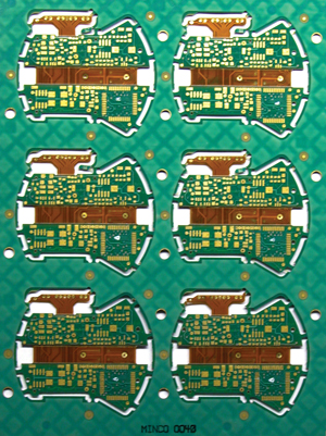
Don’t specify a pallet size without contacting your circuit vendor. In many cases, additional assembly such as component mounting will be required after the circuits are received from the flex circuit manufacturer (Figure 1). When this is true, it is desirable to receive the circuits in pallet form so that they may be processed by automated pick and place equipment. The pallet may contain one or multiple circuits depending on the circuit and pallet size. It must be sized to accommodate the limitations of the pick and place equipment, but at the same time it should be sized to have as little impact as possible on the bare circuit manufacturing processes.
|

FIGURE 1. Many applications require that the circuits are shipped in pallet form to aid in component assembly. It is important to ensure that the pallet is sized to fit efficiently on the manufacturer’s processing panel.
|
Most flexible circuits are processed in panel form, and different vendors use different panel sizes to best utilize their processing equipment and techniques. If a pallet size specified by the designer does not fit well on the manufacturer’s processing panel, it can have a significant impact on the number of circuits the manufacturer can place on a panel. This will have a direct impact on the final cost of the bare circuit.
For instance, if the number of circuits per processing panel drops by 50%, the circuit cost will almost double. If a manufacturer processes circuits on a 12" x 24" panel, and the designer specifies a 12" x 14" pallet, almost half of the processing panels will be scrap since only one pallet will fit on a processing panel.
Always keep in mind that two of the biggest cost drivers of flexible circuitry are layer count and circuit size. Specifying an awkward pallet size will have the same impact as making the circuit much larger. Some flex circuit designs will allow the circuits to be palletized after they are removed from the processing panel. This allows the flex circuit manufacturer to optimize the processing panel density, and still ship the pallet size desired by the assembler. For this reason, it is important to discuss palletized designs with the flex circuit manufacturer to accommodate all requirements for the lowest possible cost.
Design
Don’t put vias in a bending area. When routing the conductors, there are many features that can be incorporated on a rigid PCB, but should be avoided on a flexible circuit. Most of these “don’ts” have to do with features that will cause discontinuities in a bending area. When a flex circuit is bent or flexed, there are stretching and compressing forces present in the bending area. These forces can concentrate anywhere there is a discontinuity in materials or construction and can lead to fractures in the conductors or insulation.
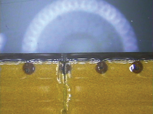
A good example of feature that would cause a discontinuity would be a via (Figure 2). A via is basically a hole in the circuit that will be weaker than the surrounding area when the circuit is bent. This weakness will tend to draw the bend towards the center of the hole. When the circuit is bent, the insulation material over the outside of the via will be subjected to extreme stretching forces which can easily result in cover film cracks. If cracks form in the cover material over a via, they will almost always propagate outward from the via and eventually through surrounding conductors.
|

FIGURE 2. Vias can act as stress concentration points when they are placed in a bend area. The figure above shows the result of five bend cycles. The crack in the cover has propagated through the silver plane layer and into the conductors below.
|
Don’t change conductor width or direction in a bend area. In an optimum flex circuit design, all conductors will be of uniform width and will cross the bend area perpendicular to the bend. This does not mean that there cannot be a 0.010" line and a 0.030" line side by side. It just means that each line should not change width in the bend area. Also, a change of direction of a conductor in a bend area can potentially cause a stress concentration point and should be avoided.
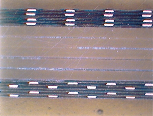
Don’t stack conductors on multiple layers. When there are similar conductors on multiple layers, they should not be stacked on top of each other. Doing so will increase the overall circuit thickness and create an “I-Beam” effect. Many board designers like to run signal and return lines on top of each other on adjacent layers to minimize EMI. If this method of EMI reduction is used, the line pairs should be staggered to reduce the I-Beam effect (Figure 3).
|

FIGURE 3. Stacked conductors can create an “I-Beam” effect (top) making the circuit less able to withstand bending; the preferred arrangement (bottom).
|
Don’t use rigid-flex construction if a multilayer circuit with stiffeners will do the job. Rigid-flex construction combines rigid PCB technology with flex circuit technology. While there are many applications that require rigid-flex construction, there are just as many that could be served equally well by a multilayer flex with stiffeners.
Rigid-flex construction can easily cost two or three times as much as a comparable multilayer, so it is important to make sure that it is only used when necessary. The most common legitimate use of rigid-flex construction is when there are rigid portions of the circuit that have SMT components on both sides of the board. If all SMT components are on one side, or there are only through-hole components, such as connectors, a multilayer flex with stiffeners will most likely do the job for a lot less money. If in doubt on whether an application should be rigid-flex or multilayer flex, it is advisable to contact a flex circuit manufacturer for guidance prior to starting the design.
Don’t use sharp inside corners on the circuit border. Flexible circuit materials are reasonably tear resistant, but once a tear starts, it will tend to propagate. A sharp inside corner on the circuit outline is a prime location for a tear to start since it can act as a stress concentration point if the circuit is flexed in that area. For that reason, it is advisable to radius all inside corners a minimum of 0.030" on the circuit outline. If space allows and the inside radius can be increased to 0.060"-0.075", do it. The larger the radius, the less chance there will be for a tear to start in that location.
Assembly
Don’t use a heat gun to heat form flex circuits. It is a well-known fact that heat will soften a flex circuit and make it easier to bend. While heat can make the forming easier, it is important to ensure that the heat source will not over-stress the flexible circuit. A heat gun is capable of extreme temperatures that are well above the maximum temperatures a flex circuit can tolerate. Also, it is virtually impossible to regulate the temperature since it is a function of the heat gun setting and the distance the flex circuit is from the nozzle. Even at a low setting, a heat gun can produce high enough temperatures to blister and delaminate a circuit if it is placed too close to the nozzle.
Don’t use rigid PCB temperature profiles to reflow flex or rigid-flex PCBs. Most flexible circuits are constructed using layers of polyimide film dielectric and copper foil bonded together with modified acrylic adhesive film. These materials provide the properties that allow the circuit to bend and flex while also providing electrical isolation between layers. The shortcoming of this construction is high moisture absorbing properties and low tolerance to elevated temperatures. While the polyimide film can tolerate very high temperatures, the acrylic adhesive cannot (service temp of 125?C). A reflow oven temperature profile for a multilayer rigid PCB will most likely be way beyond what a flex circuit can tolerate. The most obvious signs of excessive temperature exposure will be blistering and delamination. It is advisable to contact a flex circuit manufacturer that also does assembly work for guidance on proper reflow temperature profiles.
The low tolerance to elevated temperatures can be further aggravated by trapped moisture. Flexible circuits are extremely hygroscopic and can saturate in well under an hour if exposed to high humidity. To make matters worse, it can take many hours of baking to drive all the moisture from a thick circuit. When flex circuits with high moisture content are exposed to reflow temperatures, the moisture in the circuit turns to gas and rapidly expands. This can easily cause massive delamination and blistering. For this reason, it is imperative to thoroughly bake flex circuits immediately prior to reflow. If the circuits are baked more than 30 minutes prior to reflow, they should be stored in a sealed desiccant box until they are placed in the reflow oven.
Don’t hesitate to call a reputable manufacturer during the design process. Each year, a flex circuit manufacturer will see hundreds or thousands of new flex designs. This experience gives them a unique insight to what works, and just as importantly, what does not work when designing, fabricating and assembling flexible circuits. Tapping into this knowledge base will give the designer a better chance of incorporating the right design features by not incorporating the wrong ones. PCD&M
Mark Finstad (This email address is being protected from spambots. You need JavaScript enabled to view it.) is principal applications engineer for the Flex Circuit Division of Minco.


