
Twenty-nine steps to reducing issues prior to simulation.
Power is one of the most important challenges in designing printed circuit boards. Power requirements depend on the application, be it medical equipment, automobiles or consumer electronics. Power integrity is the analysis to check whether the desired voltage and current from the source gets delivered to the load.
This includes simulation to validate whether the power distribution network (PDN) maintains a proper DC voltage level at the loads, and the impedance between power and ground is minimal for the appropriate frequency range, so it is well below the target impedance.
It is essential to have design practices implemented first-hand to ensure better power integrity, rather than fixing issues at a later stage of design or manufacturing. Following is an overview of PCB layout and schematic design practices that should be performed prior to releasing the design for checks. Power integrity simulations can be performed for verification afterward with the help of simulation tools.
To understand the power flow, review the schematics for information, such as power block diagram, power budget chart, amperage of power rails, identification of main input power rails to the board, identification of other power rails converted from main power rails, etc. (FIGURES 1, 2 and 3).
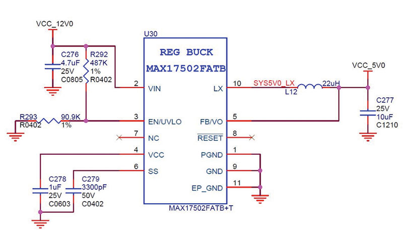
Figure 1. Schematics for power supply.
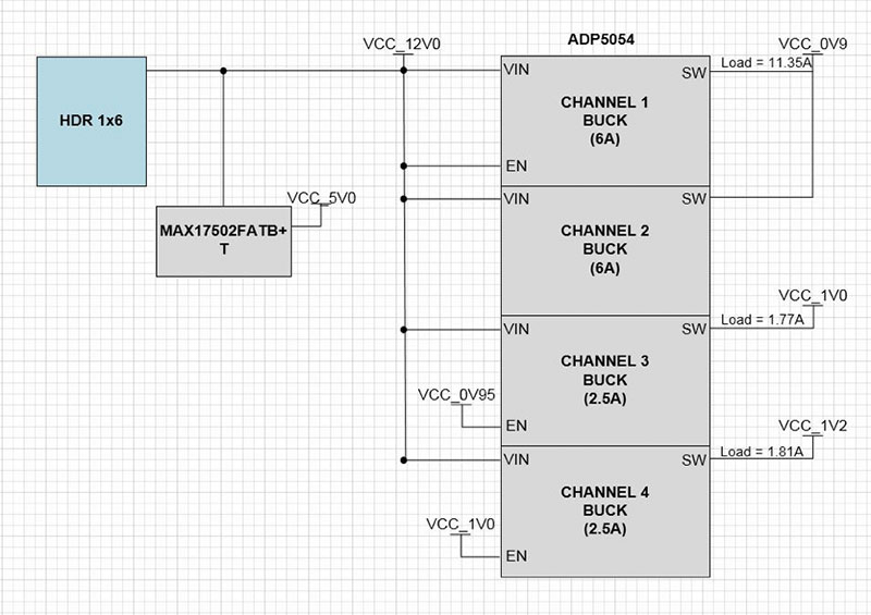
Figure 2. Power block diagram.
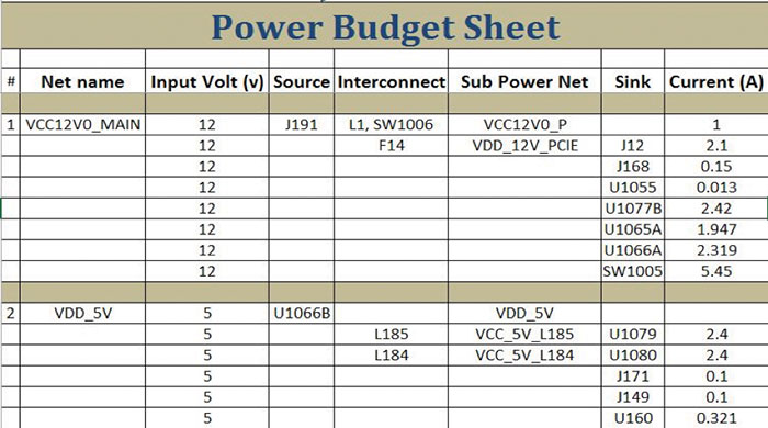
Figure 3. Power budget chart.
Read the notes added in schematics by the designer for any relevant information. Study the data sheet of the main chip of power supply for schematic and layout design recommendations and implement them accordingly, as they supersede all general practices.
Make sure all power supply components are placed on the same side if possible. If layout is congested, components may be placed on both sides.
Bypass capacitors to be placed next to input and output pins of power supply chips are provided in their data sheets. Otherwise, 10µF and/or 22µF may be selected, if not specified.
Small value caps should be placed close to the respective pins of the main IC for power supply. Usually, the smallest value cap is placed exactly on/underneath the pin, and then next to it are the larger ones, and so on. Bigger decoupling caps may be placed faraway but within their voltage planes.
Input and output components of the power supply should be placed separately.
Today, most designers draft schematics such that power-supply components shown are in the same sequence as required in the layout. Hence, power-supply components in the layout should be placed in the same flow or sequence as shown in the schematics.
As much as possible, use thick traces for all nets of the power IC chip. Moreover, intra power-supply routing should be short, direct, straight and isolated from the rest of the signals. Thus, power-supply components should be placed with this rule in mind.
Recommend the schematic circuit designer select ferrite beads, inductors with low DC resistance for low dropout. Also, the current rating of the inductor should be greater than the actual current that will pass through it.
Place power supplies close to their load IC to reduce the voltage drop caused by the loss due to the longer copper plane medium path.
If there are analog and digital sections in the design, keep them apart by placing analog and digital power supplies in their respective sections. ADC or DAC should be close to their respective power plane area.
Generally, values of bypass caps to be placed next to load chips are recommended in the data sheet, which are pre-calculated. However, the voltage rating of the capacitor selected should be at least double the voltage of the power rail. Bypass caps are frequency-dependent, but a combination of 0.1µF, 4.7µF and 10µF caps may be used if not specified in the data sheet. There is a frequency response curve based on these values if precise selection is desired.
A rough estimate is to have one cap per power pin for decoupling. The precise number of caps required can be obtained by performing power AC simulations using simulation tools.
Place small-value bypass capacitors as close as possible to the power pins of load chips for effective decoupling.
Big caps should have at least two vias per pin. Similarly, the number of vias at input/output of filter circuits like ferrite beads and inductors should be at least two or more, depending on the current.
Input and output pins should have shapes on both top and bottom layers. This applies to switching regulators, LDOs (low dropout regulators), power modules (bricks), PMIC (power management integrated chip), POL (point of load), etc. These shapes should then be stitched with a sufficient number of vias to the respective planes (FIGURE 4).
Figure 4. Power supply shapes.
Shapes should be large enough to be able to handle the specified amperage of the power voltage rail. Check the size of shape/trace for any power rail with the help of any trace width calculator/utility, according to the current rating requirements (FIGURE 5).
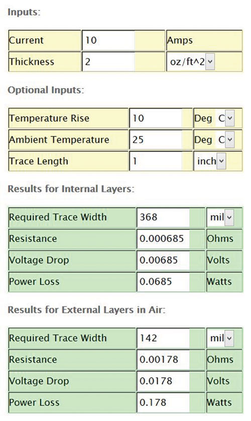
Figure 5. Trace width calculator.
Depending on design requirements, a minimum of 1 oz. copper thickness is normally recommended for power and ground (GND) plane layers.
Ground shapes are to be made according to input/output power shapes, and the vias of similar number to that of power shapes.
Vias should be added according to amperage of power rail. Assume one via per amp for a 12mil via drill. It may be calculated precisely with the help of a via current calculator/utility.
Check for bottle-necking in power plane paths, especially split shapes. For optimization, better flow and providing more copper to power plane shapes, edit shapes accordingly or move vias or relocate discretes. This can be done by changing via patterns if much of the shape is eaten by voids. Ideally, place caps in such a way that their vias follow a pattern that will void the longer side of the shape rather than the shorter side (FIGURES 6 and 7).
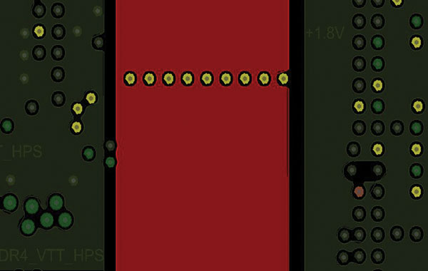
Figure 6. Bottle-necking.
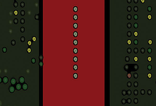
Figure 7. Removal of bottle-necking after optimization.
Chamfer the corners of power/GND plane shapes to 45° rather than 90° for better smooth current flow and to avoid the possibility of spikes at sharp corners (FIGURES 8 and 9).
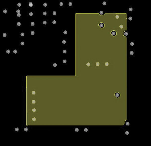
Figure 8. Shape corners at 90°.
Figure 9. Shape corners and chamfer at 45°.
Check that reference planes (adjacent planes) are not being eaten up for signals, especially critical or impedance-controlled signals. Use/maintain the “low loop inductance” method for fan-out of bypass caps by placing vias close to each other and on the same side (FIGURES 10-13).
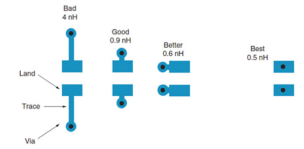
Figure 10. Recommended power fan-out pattern for bypass caps. Vias should be dropped on the sides of cap and not at ends of cap. Also, via-to-pad distance should be 5 to 6 mil air gap. Here are few examples of correct fan-out pattern.
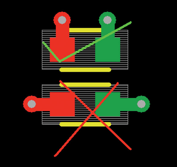
Figure 11. Current return path should be as short as possible for low loop inductance.
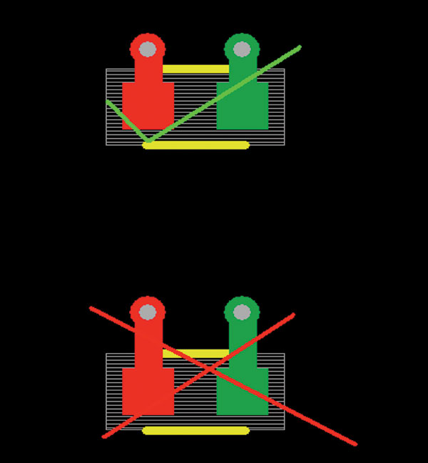
Figure 12. Pin-to-via distance should minimized, and not more than 5 to 6 mils.
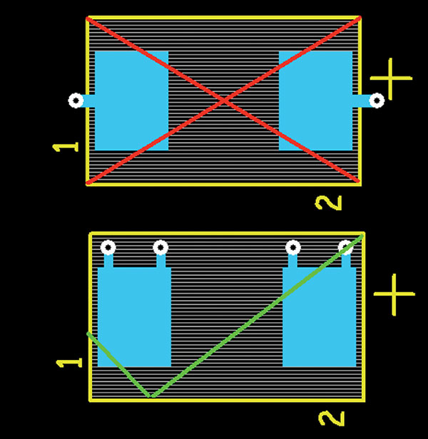
Figure 13. Bulk caps must have two fan-out vias for each pin and should be on same side, near the pin field.
Use thick traces for fan-out of all power/GND net pins. Add property in layout accordingly to check for violations by design rule checks (DRCs).
Use spokes to connect through-hole pins to power and GND planes for thermal cooling after soldering (FIGURE 14).

Figure 14. Through-hole pin connection with spokes.
Take special care of the sense resistor, as there are different ways to handle it. Normal practice is to place the sense resistors at the far end of the board. However, some designers like to place them close to the power supply’s respective pins and then route all the way up to the respective load by taking the power and GND side of resistors together in a differential pair fashion and terminating both power and GND traces under or near the respective load. Keep in mind the power and GND via near the resistor must be disconnected by voiding the respective plane manually and attaching it under or near the load (FIGURE 15).
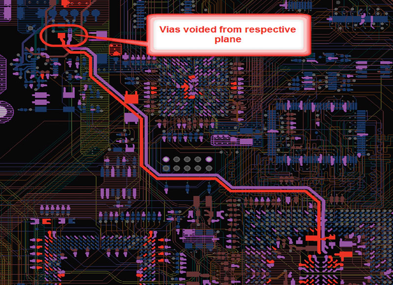
Figure 15. Sense resistor location example.
Last but not least, perform power integrity simulation, including power DC (IR drop, plane current and via current analysis) and power AC analysis (capacitor optimization) using tools and techniques for verification (FIGURES 16-19).
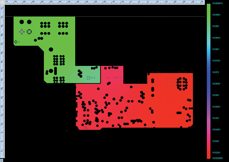
Figure 16. Voltage distribution plot.
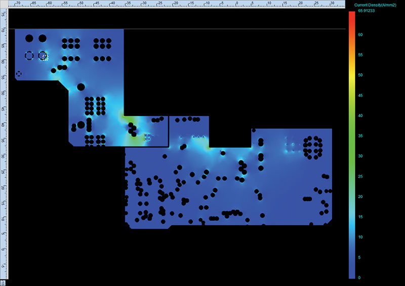
Figure 17. Plane current density plot.
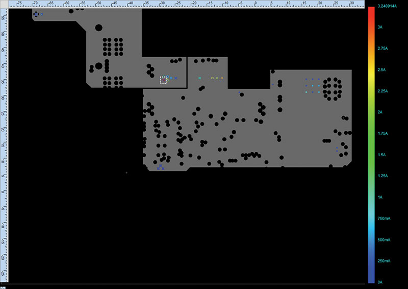
Figure 18. Via current plot.
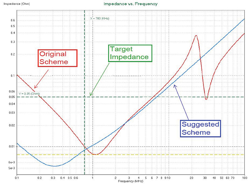
FIGURE 19. Power AC analysis_Impedance plot.
Implementing design practices early on reduces the hassle of rework during the final stages, which may induce major changes in the design and affect the schedule of the project. If all the aforementioned points applicable in the design are attended to, then hopefully the number of issues reported by the power integrity simulation tool will be minimal. Remember: Power is crucial, as it is the driving source of any board. Design carefully.
Qandeel Sheikh is EE and manager for hardware system design, PCB design and SI/PI/thermal simulations at Whizz Systems (whizzsystems.com); This email address is being protected from spambots. You need JavaScript enabled to view it..


