-
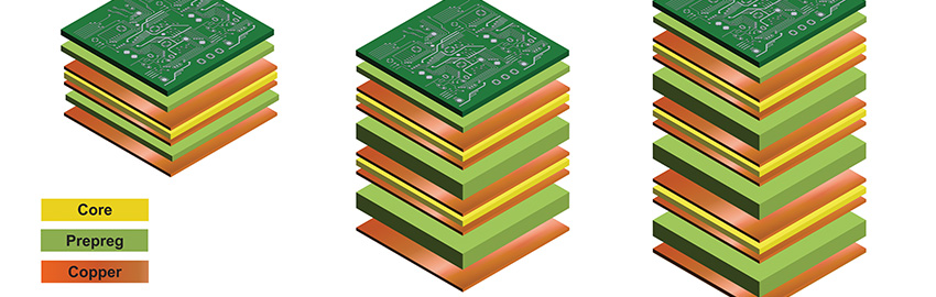
How the PCB Stackup Helps Control EMI
Power and signal placed on outer layers minimize radiated emissions.
READ MORE... -

Century Circuits
Which PCB technologies are best suited to survive 100 years?
READ MORE... -

Learning from the Past
What history can tell us about our position in high-tech.
READ MORE... -

Thermal Vias are Ineffective. Here’s Why.
Adding thermal vias can take up valuable board space with little benefit.
READ MORE... -

Connecting the Industry, from Boards to Assemblies
HDP is embarking on new rounds of evaluations of laminates and lead-free solders.
READ MORE...
Homepage Slideshow
How the PCB Stackup Helps Control EMI
Power and signal placed on outer layers minimize radiated emissions.
Century Circuits
Which PCB technologies are best suited to survive 100 years?
https://pcdandf.com/pcdesign/index.php/current-issue/241-designer-s-notebook/18061-century-circuits
Learning from the Past
What history can tell us about our position in high-tech.
https://pcdandf.com/pcdesign/index.php/current-issue/262-material-gains/18062-learning-from-the-past
Thermal Vias are Ineffective. Here’s Why.
Adding thermal vias can take up valuable board space with little benefit.
Connecting the Industry, from Boards to Assemblies
HDP is embarking on new rounds of evaluations of laminates and lead-free solders.


 Five rules of thumb for getting it right.
 As chips get smaller, the package designers are getting creative in their effort to make room for component leads. Texas Instruments’ new X2SON package sports triangular footpads in a pattern that I’m not sure I’ve seen before. X2SON stands for extra small outline no-lead. In my experience, TI is one of the better companies insofar as testing and documenting manufacturability is concerned. The datasheet for this device (ti.com/lit/an/scea055/scea055.pdf) is no exception.
 ). Imagine the TRUE (
 ) and COMPLEMENT (
 ) outputs are adjacent balls on a fine-pitch BGA, fanned-out to innerlayers. Whatever else you do, keep the trace lengths to fan-out vias equal, and keep the lengths after those vias equal until you start the parallel trace pattern. That parallel trace pattern is the coupled section because there’s electromagnetic coupling between the two sides.
