Why, relatively speaking, wider traces are quicker than narrower ones to reach the fusing temperature.
In a previous paper1 the authors explored the relationship between trace currents and temperatures. Using IPC-21522 as a starting point, we used a computer-based simulation tool (TRM – Thermal Risk Management3) to validate the IPC curves and then adjust them for a variety of typical conditions found on circuit boards. The fundamental question in these analyses is, How big does my trace have to be to carry the required current with an acceptable rise in temperature?
But these analyses typically apply to steady state currents. On the other hand, what if a trace normally carries a nominal current, but then, under catastrophic failure conditions, is subject to a severe overload? It may be necessary for the trace to be able to carry that overload for a short period of time — maybe one second or so — while the system shuts down in a controlled manner. A controlled shutdown may be necessary to prevent further system damage, or perhaps to prevent human injury. Then how big does a trace need to be?
This is often referred to as a “fusing” question, and the first two people credited with looking at this question were W. H. Preece (in the 1880s) and I. M. Onderdonk.4 There is an equation credited to Onderdonk, appropriately referred to as Onderdonk’s Equation, that relates the fusing current a trace can carry, the cross-sectional area of the trace, and (importantly) time. “Fusing current” in this context refers to the conductor current needed to raise trace temperature to the melting point of copper (1083˚C). “Fusing time” in this context refers to the time it takes to raise the conductor temperature to the melting point.5 Onderdonk’s equation is shown in Equation 1:
[Eq. 1]
where I = the current in amps
A = the cross-sectional area in circular mils6
S = the time in seconds the current is applied
ΔT = the rise in temperature from the ambient or initial
state
Ta = the reference temperature in ˚C
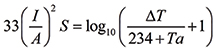
Thermal model of fuse. Details of how to utilize TRM for thermal modeling and simulation of traces can be found in the articles referenced in Brooks and Adams.1 Onderdonk’s Equation applies to a bare conductor under adiabatic conditions: that is, without the transfer of any heat into the surroundings. Since TRM is not designed to model a single layer structure, we modeled a copper PCB “fuse” as shown in FIGURE 1.
Figure 1. Fuse model for simulation.
The “board” outline dimensions are the same as the conductor. The conductor (a) was modeled as a 1 oz. (0.5 oz. on each layer) or 2 oz. (1.0 oz. on each layer) trace, 5.0mm (approximately 200 mils) long. There were pads on each end for current. The width was variable; several different widths were modeled. In all, five different configurations were modeled: 1 oz. and 2 oz. traces, 20 mils, 100 mils, and 200 mils wide.
It is important to note that Onderdonk’s Equation assumes no cooling effects – none from conduction, convection or radiation. Therefore, we minimized all cooling effects in the TRM model.
Before we look at the results, it is convenient to convert Onderdonk’s Equation to a form that is more comfortable. We start with Eq. 1 and solve for time:
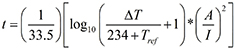
[Eq. 2]
In this equation, A is still in units of circular mils. If we assume a reference temperature of 20˚C, a fusing temperature of 1083˚C, and convert this to square mils, the result is:
t = .0346*(A/I)2 [Eq. 3]
The results for the simulation of a 1 oz., 100 mil wide fuse are shown in FIGURE 2.
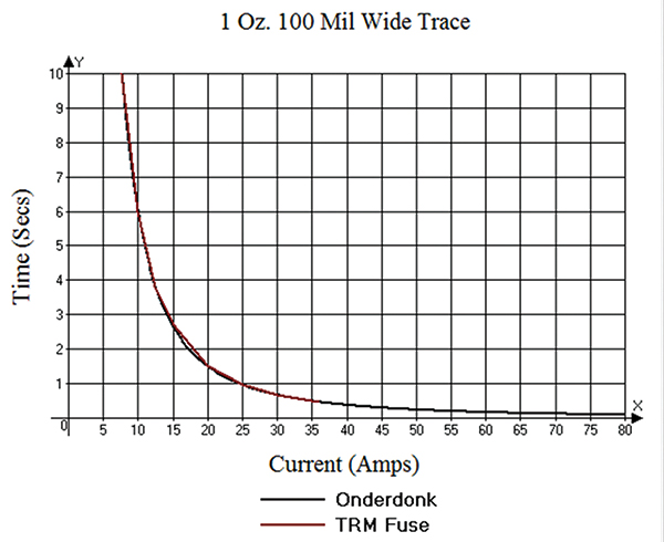
Figure 2. Comparison of fusing model to Onderdonk’s equation.
The fit is almost perfect at all levels of current. The results for all other configurations are identical to this one except for scale. This gives us a high degree of confidence in TRM’s ability to simulate a fuse in this kind of simulation.
Thermal model of a trace. We modeled a PCB trace as a 6" trace roughly centered on a board that was a 165mm long by 1.6mm thick (6.5 x 0.063") FR-4 board in still air.7 The width of the board extended 3mm on each side of the trace. The width and thickness of the trace were matched to the dimensions of the fuse model for each of six simulations.8 FIGURE 3 is an image from TRM showing one configuration of the trace.
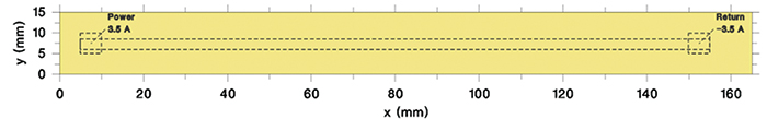
Figure 3. Model of a 6” 100 mil wide PCB test trace.
The result of the 1 oz., 100 mil wide simulation is shown in FIGURE 4. The figure shows the results of the simulation (TRM Trace), along with Onderdonk’s Equation. The significant shift of the trace model simulation to the right of Onderdonk’s Equation is primarily the result of conduction of heat into the board material, thereby slowing the increase in temperature. There is a slight cooling by convection into the surrounding air, but the timeframe is so short that this effect is relatively minor. An interesting observation of this result is that at relatively high current (and therefore at relatively short time) the curves begin to merge. This is the area where the cooling effects of the board dielectric material have not had time to “kick in.”
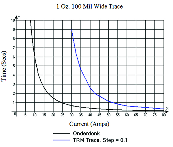
Figure 4. Simulation of a 6" 100 mil wide, 1 oz. trace on FR-4 in still air.
Short-term implication. Let’s look back at Eq. 3 (for Onderdonk’s Equation) and rearrange terms:
t (I/A)2 = .0346 [Eq. 4]
This says the product on the left is a constant.9 When we plot the same term (t (I/A)2) for the trace model simulations (again, see8), we get the interesting result shown in FIGURE 5.
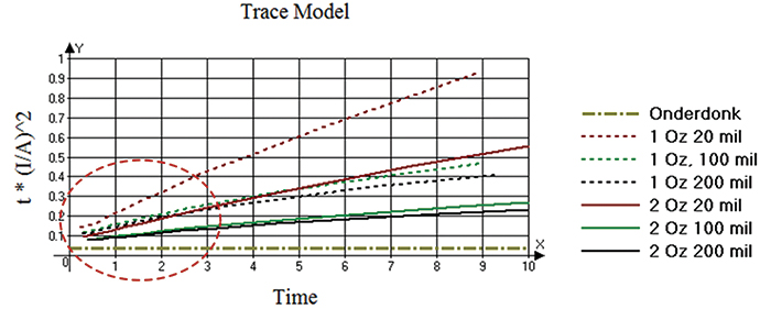
Figure 5. Plot of t*(I/A)2 for the various configuration simulations of the trace models.
They are all upward sloping to the right, a clear indication of the cooling effects taking place with time.
But when we look closely at these same curves at very short times, they all seem to originate at a value near the value calculated from Onderdonk’s Equation (0.0346) (FIGURE 6). Therefore, at the first instant of time, all the trace configurations seem to start out the same. Furthermore, except for the smallest trace (1 oz., 20 mils), they are all at or under 0.25 during the first three seconds.
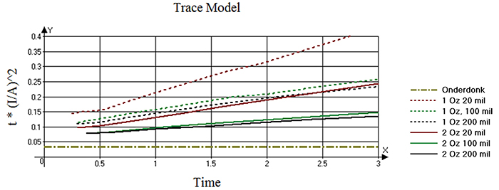
Figure 6. Plot of t*(I/A)2 for the various configuration simulations of the regular traces at times up to three seconds.
It is instructive to compare the fusing current for the traces at various times to the fusing current calculated from Onderdonk’s Equation. We calculate the ratio of these two values and provide them in TABLE 1.
Table 1. Ratio of Trace Model Current to Onderdonk Current
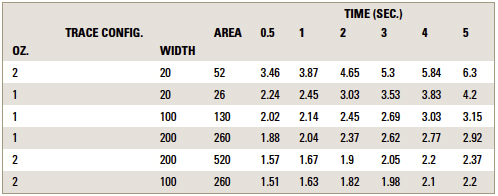
To use this table in a practical application, follow these steps:
- Calculate the trace area for your trace.
- Calculate the fusing current for the desired time (or the time from the desired fusing current) using Onderdonk’s Equation.
- Select the closest row for your combination of width and area.
- Find the multiplier for Onderdonk’s time for that row.
- Multiply the current from Onderdonk’s Equation by that multiplier to determine the fusing current for your trace at that fusing time.10
Note the simulation here allows for convective and radiative cooling from the trace. But these effects are relatively minor during the timeframes studied here. The predominant cooling effect is conduction through the dielectric material. We sampled a couple other conditions:
- Increasing the board width had no effect on fusing time.
- Adding a plane to the underside of the board had no effect on fusing time.
- Changing the material (for example to polyimide) will permit slightly better cooling and increase the fusing time somewhat.
- Adding a plane 12 mils below the trace layer did have a significant effect on fusing time, from around 33% to over 100%, depending on the level of current. (Smaller currents, and therefore longer fusing times, saw a greater percentage increase in fusing time in the presence of a plane directly under the trace.)
A very interesting result here is that, relatively speaking, narrower traces take longer to reach the fusing temperature than do wider traces. That seems, on the surface, to be counterintuitive. But the narrower traces do cool better. Narrower traces have a smaller dielectric area directly underneath the trace, relatively speaking, than do wider traces. Therefore, narrower traces can “shed” heat to the dielectric outside the trace area better than can wider traces.
Conclusions
Looking at the question of fusing currents on PCB traces can be very problematic. Onderdonk’s Equation is a reasonable place to start, and thermal simulation models suggest the actual fusing currents can be 1.5 to 6.0 times larger than Onderdonk suggests (and more, considering the restrictive assumptions of the models). But many subtle variables are involved. It is not really practical to solve this type of problem with a formula or graph. The use of a simulation model is almost required, even more so if there are adjacent traces or planes that can contribute to trace cooling.
And a word of caution: If a trace fuses, it is never acceptable to repair the trace and put the board back into service. If a trace fuses, that is considered a destructive failure and the board must be removed from service. The heat from the fusing temperature may have caused any number of hidden potential problems in the material and components around that area. It may be useful to use a trace as a fuse, but doing so is a one-time event. If a replaceable fuse is required, a fusing component must be used instead.
References
1. Douglas G. Brooks, Ph.D. and Johannes Adam, “Trace Current/Temperature Relationships,” PCD&F, June 2015. A more comprehensive analysis, “Trace Currents and Temperatures Revisited,” 2015, is available at ultracad.com.
2. IPC-2152, “Standard for Determining Current Carrying Capacity in Printed Board Design,” August 2009.
3. The software tool we use is called TRM (Thermal Risk Management), developed by Dr. Johannes Adam. See adam-research.com for more information regarding the tool and these types of simulations.
4. Douglas G. Brooks, Ph.D., and Johannes Adam, “Who Were Preece and Onderdonk?” PCD&F, July 2011.
5. A certain amount of time is required, let’s say T1, to heat the conductor to the melting point (referred to in this article as “fusing temperature”). An additional amount of time is required, let’s say T2, to convert the conductor from a solid to a liquid. In this article, “fusing time” refers to the first time, T1.
6. A circular mil is the area of a circle with a diameter of one mil. The formula is A = d2. The conversion from circular mils to mil2 is π/4. Normal conversions are:
1 mil2 = 1.273 circular mils
1 circular mil = .7854 mil2
1 m2 = 19.736*108 circular mil
1 circular mil = 5.067*10-10 m2 = 5.067*10^-4 mm2
7. The Heat Exchange Coefficient, see Ref [1], was set to 10. However, the result is not sensitive to a change in this coefficient.
8. Results and comparisons for all six simulations can be found at Brooks and Adam, “Fusing Currents in Traces,” ultracad.com.
9. Furthermore, if we let A = constant, then Equation 7 reduces to I2t = constant. The I2t value is an important rating in the fuse industry. See http://en.wikipedia.org/wiki/Fuse_%28electrical%29#The_I2t_value.
10. UltraCAD’s trace calculator UCADPCB4 can do these calculations.
Douglas Brooks, Ph.D., is owner of UltraCAD Design, a PCB design service bureau and author of PCB Currents: How They Flow, How They React; This email address is being protected from spambots. You need JavaScript enabled to view it.. He will speak at PCB West in September in Santa Clara, CA. Johannes Adam, Ph.D., CID, is founder of ADAM Research, a technical consultant for electronics companies and a software developer, and the author of the Thermal Risk Management simulation program.