Power and signal placed on outer layers minimize radiated emissions.
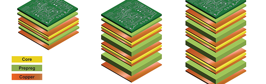
The PCB stackup is like a building's foundation; a product not built on a strong base will fall apart. When electromagnetic compatibility (EMC) testing is considered, the PCB stackup is a major determinant of radiated EMI, and to some extent, conducted EMI. A PCB stackup design that enables low EMI also aids signal integrity and power integrity, as all these areas are linked and must be considered in totality.
So, to ensure a PCB design passes EMC testing, understand the stackup's role in generating emissions and determining EMI susceptibility. Simple changes in materials, layer assignments, and routing strategies can make the difference between passing and failing EMC tests. All these decisions originate in the PCB stackup.
A special panel discusses the growth of AI tools and its possible effects on the industry.
“Will AI take my job?”
That’s the question on the mind of many around the world today – including electronics engineers and PCB design engineers – and was one of several questions considered during an online panel hosted by PCEA in March.
A group of panelists with notable AI experience – Circuit Mind’s Tomide Adesanmi, Cadence Design Systems’ Taylor Hogan, Zuken’s Kyle Miller, Luminovo’s Sebastian Schaal and Siemens Digital Industries’ David Wiens – gathered to share predictions for the future of AI in the electronics supply chain and answer questions from an audience of industry professionals.
HDP is embarking on new rounds of evaluations of laminates and lead-free solders.
The High-Density Packaging User Group, the nonprofit consortium of electronics manufacturers and suppliers that collaborate on various technical problems in order to reduce cost and time to market, has nearly 25 projects underway, several of which are due to be completed this year.
We spoke in March with Madan Jagernauth, marketing director and project facilitator of HDP, about its current research on lead-free solder alloys, its recent conference Best Papers, and whether the consortium members are ready to tackle artificial intelligence.
Written by Douglas G. Brooks, Ph.D. and Dr. Johannes Adam
Category: Features
Adding thermal vias can take up valuable board space with little benefit.
We have developed several articles and publications in the past questioning the value of thermal vias.1 Here is our definitive conclusion, and why.
Thermal vias are non-current-carrying vias between two layers provided for the purpose of permitting heat to conduct from one layer in a PCB to another. The idea is to lower the temperature of the heated surface compared to another, lower temperature surface. In a typical application, the heated surface might be a pad underneath a heated component. The opposite surface might be another pad or plane further down in the PCB structure. Someone untrained in heat transfer might suggest using thermal vias without an opposite copper surface, but we will show that such an approach is totally ineffective.
Building and maintaining what's said to be the world's largest CAD database requires strong relationships.
Keeping up with the increasing demand for new and specialized components is no easy task, but Ultra Librarian's team has proven up to the task – to the tune of more than 16 million components in its library and a quarter of a million unique downloads per month.
When we visited Ultra Librarian's office in Huntsville, AL, in early December, EMA Design Automation had just announced the library service's spinoff into a new ECAD-oriented company, Accelerated Designs, which was the original name of the company under its founder, Frank Frank, before it was acquired by EMA in 2016.
Written by Doug Brooks, Ph.D. and Dr. Johannes Adam
Category: Features
Coating traces or filling vias is usually a wasted expense.
We are often dismayed by the number of individuals (and especially board manufacturers) who suggest that coating a trace or filling a via cavity can result in significant thermal and/or electrical conductivity improvements. Herein we will try to explain why, in almost all cases, this is not true.
Individual trace coatings. Often users (especially board manufacturers) suggest trace thermal or electrical conductivity can be improved by coating the trace with some conducting material. It sort of makes intuitive sense that additional material can provide more benefit. Trace coatings are typically limited in a practical sense to plated copper or a solder coat. We suggest that such a coating can be analyzed by looking at the separate elements (bare trace and coating) as two parallel conductors.