Power and signal placed on outer layers minimize radiated emissions.
The PCB stackup is like a building's foundation; a product not built on a strong base will fall apart. When electromagnetic compatibility (EMC) testing is considered, the PCB stackup is a major determinant of radiated EMI, and to some extent, conducted EMI. A PCB stackup design that enables low EMI also aids signal integrity and power integrity, as all these areas are linked and must be considered in totality.
So, to ensure a PCB design passes EMC testing, understand the stackup's role in generating emissions and determining EMI susceptibility. Simple changes in materials, layer assignments, and routing strategies can make the difference between passing and failing EMC tests. All these decisions originate in the PCB stackup.
Key Elements in PCB Stackup Design
For experienced designers, stackup design isn't terribly complex, even for designs that require high-speed routing or RF interconnects. From an EMC perspective, effectively managing EMI and reducing susceptibility hinges on a few key parameters:
- Strategic placement of ground within the PCB stackup
- Utilization of planes for power and ground
- Appropriate dielectric thickness between signals and ground
- Incorporation of copper pour within signal layers.
Carefully crafted PCB stackup can effectively mitigate common EMI issues that plague new designers. In addition, by solving these EMI challenges, one can simultaneously address specific signal integrity issues, particularly those related to routing and impedance control. Now let's dig into each of the above areas to see where EMC can be addressed.
Location of Planes in Multilayer PCBs
The placement of plane layers within multilayer boards significantly affects signal integrity and EMI. In high-speed designs, it also plays a major role in ensuring power integrity. In early two-layer designs, boards relied on conductively filled vias for grounding, which were then connected back to the primary power source. Today, even entry-level PCBs for most designs have at least four layers, primarily for EMI mitigation and improved signal integrity.
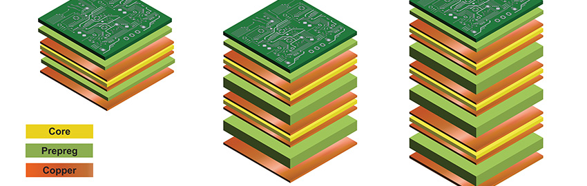
A standard four-layer stackup is shown in Figure 1. This configuration provides two internal ground plane layers, ensuring effective shielding for all signals on the outer layers. This concept can be easily extended to six layers, eight layers, and beyond.

Figure 1. PCB stackups with four layers, six layers, and eight layers.
Placement of power and signal on the outer layers is preferred for minimizing radiated emissions. This configuration permits placement of an adjacent internal ground plane or image plane beneath any switching elements or signals on the top layer. This significantly reduces radiation from these elements.
Other advantages of placing a ground plane in close proximity to signals include reduced crosstalk and streamlined impedance control. With a ground plane situated in a layer adjacent to signals, the impedance of the trace and its mutual inductance/capacitance to nearby traces can be determined. This arrangement enables designers to effectively control all three factors, allowing them to easily mitigate EMI and crosstalk without sacrificing impedance control.
2-Layer PCBs and Ground Planes
What about two-layer PCBs? Can or should they have a ground plane?
In two-layer board designs for digital systems, establishing a ground plane is generally recommended. The use of two-layer boards for digital systems is acceptable under the following two broad conditions:
- When component placement and routing density is low
- When the system doesn't involve fast signals (those faster than 1ns).
The first condition is important since it dictates the feasibility of grounding by copper pour and stitching vias. As component density and the number of traces increase, there's limited space for copper pour on the top and bottom layers. Consequently, the ground becomes poorly defined near digital signals, potentially leading to increased radiation. It is also more difficult to maintain consistent impedance across the entire interconnect, especially differential impedance.
The result is a board that resembles the image in Figure 2, which readers may recognize as an Arduino with dense, high-speed routing near the USB connector and headers.

Figure 2. Arduino boards with dense, high-speed routing near the USB connector and headers typically pass EMC testing.
While Arduino boards typically pass EMC testing, it is important to note that design practices employed in Arduino boards do not universally apply to other digital systems.
The second condition is crucial since signal speed directly impacts the level of radiation emitted. Faster signals inherently emit more radiation, particularly at higher frequencies where the power spectrum concentrates more energy. This demands increased grounding to effectively suppress radiation. For this reason, it is common practice to use four-layer boards, at minimum, for PCBs designed to send and receive high-speed signals.
Layer Thickness
The thickness of the dielectric between signal and plane layers determines several parasitic effects, which are important determinants of EMI and signal integrity (SI):
- Trace self-inductance
- Trace self-capacitance
- Trace mutual-capacitance
- Spreading inductance for planes and pours.
The first two items in the list directly impact both EMI susceptibility and the level of radiated emissions expected from a PCB stackup. Furthermore, capacitance, whether self or mutual, plays a crucial role in capacitive coupling of noise originating from other conductors in the system, such as the enclosure. This coupling may lead to the undesirable occurrence of common-mode noise coupling/infiltrating an interconnect.
One fundamental parameter in PCB stackups that directly influences all the aforementioned parasitic effects is the thickness of the dielectric layer separating signal-carrying conductors and a ground plane. Similarly, the distance to a uniform power plane, acting as the reference for a trace, is vital. By bringing the reference layer closer to the signal layer – accomplished through use of a thinner dielectric – radiation and coupling, which lead to noise currents in copper traces, are reduced. This applies regardless of the circuit type (power, digital, RF, etc.).
What About Radiation from Rails and Planes?
For power integrity and radiated emissions, particularly where rails are concerned, the key consideration lies in the nature of these conductors. Large rails, such as those used for power distribution, essentially carry DC power overlaid with an AC signal (voltage ripple). In the case of digital systems, rails supply pulses of current to power-hungry processors. In both cases, the AC portion of the delivered power generates a changing magnetic field, which manifests as radiated emissions.
The spreading inductance of these large conductors dictates the amount of radiation. Essentially, what we call self-inductance for traces is equivalent to spreading inductance for a large polygon-shaped conductor. The main difference is that the spreading inductance is determined by the region in the conductor where current exists. Therefore, spreading inductance determines radiated emissions, while self-inductance in planes determines susceptibility.
The easiest way to reduce both factors in a PCB stackup is to bring the ground plane closer to the copper pour region used for power distribution. This approach reduces both spreading inductance and self-inductance, thereby confining the electromagnetic field within the stackup to reduce radiation. In terms of power integrity, this proximity increases plane capacitance, which proves beneficial for stable power delivery even at high frequencies up to gigahertz.
The Fabricator, The Stackup and You
Understanding the principles of PCB stackup design, especially with regard to EMI and EMC, is paramount for any product destined for commercial success. The most important aspect of designing a PCB stackup, however, lies in ensuring it can be built at scale. This entails consideration of material availability and processing feasibility, which must be balanced against the performance or engineering requirements of the PCB and the end-product.
So, how should a designer approach selection of a stackup to ensure minimal EMI and successful EMC testing? There isn't a singular stackup blueprint that guarantees a design will pass EMC testing – multiple designs can achieve the same goal. It's more important to understand the key parameters that can be adjusted in a stackup, rather than starting from scratch with every design iteration.
Your fabricator will inevitably have valuable input regarding the stackup, particularly regarding available materials and layer thicknesses in the stackup design. Therefore, involving the fabricator in the stackup design process is essential. Areas where a fabricator can help include:
- Determining if a standard stackup will meet project requirements
- If a custom stackup is needed, determining the optimal layer arrangement and availability of materials
- Selecting appropriate layer thicknesses from available material options
- Verifying and fine-tuning the custom stackup design, ensuring alignment with manufacturing capabilities and material availability.

Figure 3. Fabrication engineers can assist in meeting end-product requirements.
In many cases, a standard stackup with ground planes will be adequate to achieve low radiated EMI and, often, low conducted EMI. It is imperative to arrange and utilize the layers appropriately, however, lest the layer count and layer construction fall short in fully mitigating EMI issues.
Akber Roy is chief executive of Rush PCB (rushpcb.com); This email address is being protected from spambots. You need JavaScript enabled to view it..