A co-design solution for a wireless RF flip-chip design dilemma.
Toshiba faced a difficult design problem.
Its TransferJet wireless IC technology was embedded in a customer cellphone. When the next rev of the phone came around, Toshiba needed to shrink the board to 4.5mm x 6mm from 8mm x 8mm, and had to shrink the module thickness to 1.0mm from 1.7mm. The original design was a simple board with a wirebond package and several peripherals. Competitive pressures required a significant reduction in size and thickness. On top of that, RF matching had to be added to simplify adoption of the module.
The overall goals were to shrink the size and thickness, provide RF matching and power stabilization, and minimize noise. The system block diagram plus the design goals are shown in FIGURE 1.

Figure 1. System block diagram and design goals.
To accomplish these goals, Toshiba came up with the following requirements:
- Use a bare flip-chip die instead of a wirebond package.
- Embed the die in the package substrate, and add extra test pins.
- Use co-design tools and methodologies to optimize pin assignments more effectively.
- Use system-level co-analysis.
- View and edit using 3-D design capabilities.
- Design in close collaboration with CAE tools.
Toshiba chose Zuken and Ansys to provide tools to meet all the functionality requirements. Feasibility studies began. Toshiba embedded the die and explored putting it face up and face down. It also explored the effects of adding test pins. What resulted is the configuration in FIGURE 2: the die had the extra test pins; it was placed face down, embedded within the substrate, and employed ultra-thin shield coating on the package and an ultra-thin IC component.

Figure 2. Cross-section view of IC die embedded within the substrate, and adjacent components and mold, surrounded by shield coating.
The design process. The module was then combined with the board to form a 3-D chip-module-board design view. Each device had its own design rules. Zuken’s CR-8000 Design Force enabled engineers to switch design context as they proceeded through the design process. The tool allows switching back and forth between 2-D and 3-D modes during package design (FIGURE 3).

Figure 3. Views of IC package in 2D and 3D.
The IC RDL routing was done natively in an OpenAccess design environment using IC design rules, and generated mask-ready RDL routing. Package routing was completed with package design rules. Pin assignments were updated as needed to create the simplest and most optimal routing in both the die and package.
Next, a 3-D model of the system was generated. This model included IC package and board elements for a hierarchical 3-D model that was passed to Ansys for RF matching analysis. The RLC parasitics were based on a 3-D model and were passed to Ansys Q3D analysis. The circuit and analysis results are shown in FIGURE 4.
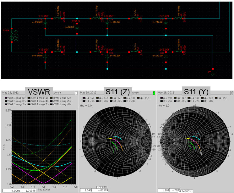
Figure 4. 3-D model of RLC parasitics.
Engineers then generated an ANF file for use in Ansys SIwave for power stabilization. A port was set for each power and ground terminal of the IC and power, and ground impedance analysis from the IC terminals was run (FIGURE 5). From this analysis, the optimum number and value of the decoupling capacitors required were calculated.
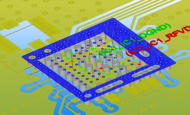
Figure 5. Ground impedance analysis and subsequent routing from the IC terminals.
In order to minimize noise, engineers performed a static resonance analysis on a 3-D model of the module (FIGURE 6). They found a strong resonance at 9GHz, and were able to find the source of the resonance. Once the resonating wire was corrected, it was time to recreate the 3D model and rerun the resonance analysis to confirm the problem was fixed (FIGURE 7).

Figure 6. Original 3-D model and source of resonance.
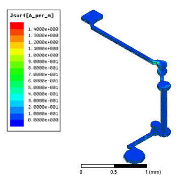
Figure 7. New model with corrected resonance.
Finally, after analyzing dynamic noise, engineers found it exceeded their constraints. So from there, they built up a series of 30 possible solutions, and ran analysis on each while applying a stimulus at the source of the noise on the IC. The software was able to identify the solution that gave the best results, reducing noise to 1/30th of the original measurement (FIGURE 8).
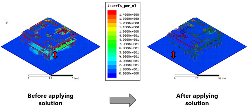
Figure 8. Dynamic noise analysis resulted in a new solution that cut noise 97%.
Now that they found good package results, they combined the module with the board for a final waveform, noise, and thermal analysis of the product and confirmed it met the requirements.
Tom Whipple is a solutions architect at the Zuken SOZO Center (zuken.com); This email address is being protected from spambots. You need JavaScript enabled to view it..


