The conference program opened on Sunday with a selection of two Design Excellence Curriculum courses, two-day programs that earn the attendees a certificate of completion and two full-day Professional Development tutorials. Topics included a program on designing for lead-free with special emphasis on the impact throughout the design, fabrication and assembly process. Instructors offered practical tools for DfM and DfA consideration. Design basics were covered, as were EMI and crosstalk for advanced designs. A hands-on tutorial offered advanced designers an opportunity to work on the design challenges of HDI/microvia integration.
All attendees convened during the Sunday luncheon to participate in a panel discussion on the topics of “The Key Components to Successful Design and Fabrication of Advanced PCBs.” I had the opportunity to introduce a few of the industry’s luminaries who offered their thoughts on the topics of advanced design, PCB fabrication and new technology implementation.
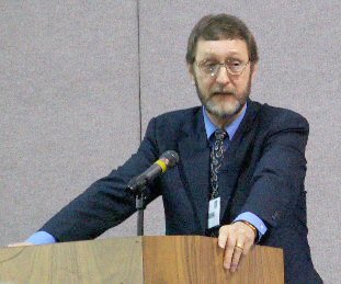
Rick Hartley, senior principal engineer and PCB specialist at L-3 Communication, Avionics Systems, was the first to speak. He brings over 30 years experience in PCB and circuit development, including signal integrity and EMI control in digital and RF PCBs. He emphasized that the design landscape is changing rapidly. The high-speed environment makes every design more challenging.
Hartley commented that before the escalation of high speed, the design was completed when there were no shorts or opens, and you had a netlist. Unfortunately, it doesn’t work that way in the high-speed world. All of the circuit functions are closely integrated so that qualifying the functionality of the design is more difficult.
Hartley stressed the basics of designing for fabrication, assembly, test and repair. He pointed out that along with the advancing state-of-the-art, there are new tools that can help in the design process. He added that the most important tool is really, “What is in your head,” because with the proper education, designers can better use the tools that are available to them.
Hartley’s conclusion was that each of us, as professionals in the PCB industry, is key to the growth and future success of advanced technology introductions. He encouraged the audience to continue to take advantage of the opportunities for education offered in programs like
PCB East and
PCB West. Being life-long learners is a prerequisite to success.

The next panelist was Happy Holden. Holden, a senior technologist with Mentor Graphics Corp., is no stranger to the fab side of the business. He retired from Hewlett-Packard in 1996 and began working with a number of companies who manufactured and sold base materials for HDI applications.
Holden’s assertion is that predictably is the key to success. In the process of designing and fabricating PCBs, every engineer is faced with an enormous number of tradeoff analyses. Many of these tradeoffs are performance driven, but an increasing number of them are also decidedly cost driven.
Part of product predictability is the question of relative costs. In the November issue of Printed Circuit Design and Fab, Holden covers this topic in depth. In his overview on Sunday, one of his assertions is that even at our current level of complexity in circuit design, the perfect tool that can mitigate the uncertainties and deliver complete predictability does not yet exist.
At its simplest form, there are five domains that interact over 25 variables in the design of a circuit board. The five domains are circuit criteria, component selection, materials, design and processes. The variables include impedance, voltage, attenuation, noise, crosstalk, number of layers, via-in-pad, breakout, design rules, via structure, overall thickness, material characteristics, HDI, surface-mount pitch, number of I/Os, component size and many more.
In reality, there are also additional domains that now significantly impact the process. Design for the environment and legislations such as RoHS and WEEE have added to the complexity of the process. In addition, electronic system co-design and E/MCAD initiatives mandate cooperative, team-driven design approaches.
Holden challenged the audience with the basic physics, chemistry and mathematics of the design process. These simple algebraic equations can provide critical insight into the importance of a particular design variable. A good example is inductance, where the thickness of the PCB factors into the equation as both a numerator and a multiplier indicating its significant impact on inductance. Understanding the equation, it’s easier to conclude that thinner PCBs have inherently lower inductance.
 Wrapping up the discussion, Mike Fitts, manager of business development at Plexus, talked about the unique challenges associated with the implementation of new products and processes into the design and fabrication process. In his presentation, Fitts focused on an individual’s responsibilities in assessing, planning for, selling and finally implementing.
 Drawing on his years of experience in new technology implementation, Fitts began the discussion with a review of the questions you need to ask before you even begin developing your implementation plan. Have you done your homework and thoroughly investigated a technology? Do you believe that the technology has some real merit? If so, how are you going to sell the technology within your company?
When the return in investment is clear, it’s an easier sell. Have you determined the ROI? Typical electronics industry ROI guidelines are two to three years. In addition to the basic financial criteria, there are additional fundamental requirements for successful technology introduction. To be able to sell the idea, you have to become the expert and the champion. From this perspective, understand the technology, its proposed benefits and also its risks. Be prepared to educate your organization on these details.
All three panelists agreed that one of the fundamental keys to success of any new project is an individual or team aptitude and preparedness. To address this fundamental requirement for education, UP Media Group looks forward to an expanded 2008 conference program; bringing educational opportunities to new regions. The conference will be in Austin in March, the Chicago suburbs in May, Santa Clara in September and Orlando in December. We all look forward to seeing you there!


 Rick Hartley, senior principal engineer and PCB specialist at L-3 Communication, Avionics Systems, was the first to speak. He brings over 30 years experience in PCB and circuit development, including signal integrity and EMI control in digital and RF PCBs. He emphasized that the design landscape is changing rapidly. The high-speed environment makes every design more challenging.
  The next panelist was Happy Holden. Holden, a senior technologist with Mentor Graphics Corp., is no stranger to the fab side of the business. He retired from Hewlett-Packard in 1996 and began working with a number of companies who manufactured and sold base materials for HDI applications.
  Wrapping up the discussion, Mike Fitts, manager of business development at Plexus, talked about the unique challenges associated with the implementation of new products and processes into the design and fabrication process. In his presentation, Fitts focused on an individual’s responsibilities in assessing, planning for, selling and finally implementing.


