To understand the influence of NFPs on reliability, industry experts were surveyed. Will their response settle the debate?
Nonfunctional pads are pads on internal or external layers that are not connected to any active conductive patterns on the layer. Figure 1 shows removal of the difference between nonfunctional pads included on and removed from a single plated via.
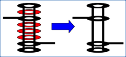
Figure 1 Schematic of NFP removal.12
DfR Solutions performed an industry survey of board manufacturers to learn the following:
* How common is the removal of nonfunctional pads from board designs by manufacturers?
* What considerations, if any, factor into the decision to remove these pads?
* Does removal have a known impact on printed board reliability?
Experimental
The survey consisted of the following. For the board described below, please answer the following questions:
* IPC Class 3 requirements.
* FR-4 (170?C) and polyimide (220?C).
* HASL finish, Sn63Pb37 only (not Pb-free).
* Thickness range: 0.020" to 0.125".
* Layer count: 16 max.
* Inner copper (oz): 0.5 to 2.0, Outer Copper (oz): 1.0 to 3.0.
Questions:
1) What is your procedure with respect to nonfunctional innerlayer pads?
2) Do you keep them or remove them as a function of board material type, overall thickness, layer count, copper thickness?
3) Is this a standard practice?
4) If you remove or don’t remove nonfunctional pads, what is the reason for doing so?
5) If you remove them, do you have reliability data you could share indicating whether there is a reliability issue?
6) Is the answer the same for epoxy-glass and polyimide board materials?
7) Is the answer the same if the circuit is high speed?
Your name: ______________________
Company: _______________________
Email address: _____________________
The survey was sent out to 22 PCB fabricators.
Fourteen US fabricators participated in the survey. An additional eight fabricators received the survey but did not respond. Of those who responded, the following paragraphs provide insight into their responses.
1. What is your procedure with respect to nonfunctional inner layer pads? To summarize the surveyed fabricators’ responses:
* Five simply remove them.
* Five would remove the pads, but typically after receiving permission from their customer.
* Four never remove them.
In addition to the fabricator survey request, DfR put a notice on LinkedIn asking for a response to this question. Only one response was received from a fabricator’s representative.
“We generally prefer to remove them unless directed otherwise to reduce AOI time. An exception (unless directed to keep them) would be if we need the additional copper for stability in lamination (if it’s a very sparse circuit layer).”
Thus, it is a standard practice for this supplier to remove them.
2. Do you keep them or remove them as a function of board material type, overall thickness, layer count, copper thickness? In all responses, the board material type, thickness, layer count and copper thickness did not alter the company’s decision to either keep or remove the unused pads.
3. Is this a standard practice? Regardless of whether the pads were kept or removed, every company responded that it was their standard practice.
4. If you remove or don’t remove nonfunctional pads, what is the reason for doing so? This question provided the most interesting responses, as it provided insight into each company’s reasoning.
Why remove unused pads?
* “The drill bit will not easily be hurt and cause hole-wall roughness. (The nonfunctional inner layer pads are also always drilled, even when the via and via hole size is small. The drill bit is also small and may easily be damaged if the copper remains for each layer.)”
* “We minimize drill wear by removing them, especially on high layer counts with thick copper.”
* “Drill life is reduced if all layers have unused lands. Drill breakage is also a concern.”
* “Removal of unused lands in wiring plane with tight registration of line-to-land requirements.”
* “To protect the drill bit from damaging and produce clean hole wall free of nodules.”
* “We remove them to reduce the opportunity of creating shorts, especially in a BGA area where typically trace/space is already fairly dense and to reduce the drill wear. The more copper we drill through, the more heat is generated, reducing the possible hit count and having cleaner holes.”
* “To enhance drill hole quality, we prefer to drill through as little metal as possible. The effect of the unused pads is to wear the drill bit more rapidly, which shows up as gouging and poor drill quality.”
* “Nonfunctional pads are normally removed to eliminate the possible misregistration perception by end user.”
* “We remove them because it allows for a better product after etching.”
* “For hole wall support on rigid product to reduce drill wear.”
Why leave unused pads?
* “In our case, concern for accidental removal of a functional pad. However, I began in business at TI, and we always removed nonfunctional pads because our concern was bond strength of the electroless copper to the internal surface copper. If you didn’t need the copper, you’d remove it. Also less chance for shorting in plane areas for nonfunctional pads.”
* “We believe that they anchor the hole and improve reliability. However, we have begun questioning this and have a DOE in progress to investigate.”
* “The more copper that can be retained on any layer, the better the dimensional stability. Providing a complete pad stack (with the exception of plane layers) has improved registration and permits proper DPA (destructive part analysis). This ability to verify registration or misregistration anywhere within the product panel provides a great benefit. The additional copper also permits better chip evacuation and prevents or greatly reduces clogged flutes.”
* “Primarily electrical test shorts and AOI callouts for shorts.”
Summary of responses. In all cases, remove or leave, the primary reason was to improve the respective fabricator’s process and yields. Companies that remove unused pads do so primarily because they want to extend drill bit life and produce better vias in the boards, which they consider the primary reliability issue. For those that keep unused pads, the primary reason is that they believe it acts as a multi-flanged rivet to combat innerlayer damage. Such delamination is the result of non-homogeneous z-axis expansion of the board due to differences in the CTE of the disparate materials.
In general, companies responding did not feel that removing the unused pads would create a reliability issue.
Reliability Data
DfR did not expect to get many responses to these questions due to the proprietary nature of the data. However, some of the responses detailed how the fabricators gather appropriate data to make their decisions.
5. If you remove nonfunctional pads, do you have reliability data that you could share indicating whether there is or is not a reliability issue?
* “We added two test coupons under the rails of the working panel (Figure 2). The test coupon includes the minimum hole size and maximum hole size and our minimum trace. The hole we designed included each layer’s pad. When we complete the 1st copper plating, our lab cross sections these two coupons and checks the hole wall roughness, copper thickness, and the layer to layer registration. If the coupon showed any layer without an annular ring, then we increase the check quantity. If the result was unacceptable, then we may check all working panels and scrap the defect boards in the PTH process. Engineering would then investigate to check if the issue happened in the inner layer process, lamination process or drill process. After finding the root cause, we correct the issue and replace the defective boards.”

Figure 2. One of two test coupons on panel.
* “This is a combination of many factors. We have seen in the past when we have a high rate of gouging (0.0007), we have multiple initiation points for plating folds that are always the first to fail. Having nonfunctional pads reduces this potential. Also, depending on construction and how resin rich the stack-up may be, we see a higher amount of lifted pads and/or actual cracking of the ED foil in the high layer count thick products that have minimal interconnects. Even though your scenario speaks about (not Pb-free) we see there are many CMs thatsubject the product into those temperature ranges, especially for selective connectors that require a solder fountain application. We did have a product for an ATE customer that had active components (slightly over your thickness, as it was 0.188"). They had multiple failures until the nonfunctional pads were re-added, and then there were no further issues. Same design, just pads vs. no pads. We have also seen more instances of larger layer count product coming in with pads removed. From an electrical standpoint, the additional capacitance is not good for signal integrity, so they are required to be removed. For this type of product, we need to make sure we increase the plated copper to 0.0015" minimum, as we saw failure with 0.0008" minimum copper thickness. We also did a reliability test with the attached pad stacks. I am not able to share the results with you due to NDA.”
* “PTH life can be affected with the addition of unused lands for “smaller” diameter vias; data are out on IST type fails. Larger PTH diameter may have improved life with unused lands, not enough data in the open.”
* “Yes, we provide TDR impedance report when impedance is requested, reliability report, and cross-section.”
* “The reliability data we would have is in the form of the IPC-6012 Class 3 requirement for the specific customer part. And what would be included in the C of C package supplied with the part. We do perform part number and material qualification through an independent lab. We typically cannot share these data.”
* “Based on customer returns or, more accurately, the lack of customer returns, the practice of unused pad removal does not adversely affect functionality or reliability.”
* “It is not a reliability issue on rigid boards. Unused pads just wear on the drills, especially those with higher layer counts and high copper weights.”
6. Is the answer the same for epoxy glass and polyimide board materials? All suppliers said that their response was the same regardless of whether polyimide glass or epoxy glass materials were involved.
7. Is the answer the same if the circuit is high speed?
* “Yes. More so for high speed because nonfunctional pads (NFPs) have a signal integrity impact on the holes (from a supplier typically removing the unused pads).”
* “No, for high speeds, these unused lands increase loss (>10Gbps) (from a supplier that typically keeps the pads).”
Rigid-flex. Several suppliers also responded that if the board were a rigid-flex configuration, they would leave the unused pads in place to provide additional reinforcement for the Kapton Mylar flex material.
Additional Insight from Industry
Technical papers and discussions that address this issue were also examined. (No company or individual who participated in the survey is cited in this section.) Impact to both design function and reliability are seen with the use of NFPs.
Industry Publications
In “Signal Integrity Analysis of a 26 Layer Board with Emphasis on the Effect of Nonfunctional Pads,”1 Ciccomancini Scogna shows that nonfunctional pads consistently impact insertion loss. Insertion loss provides information about both the quality of the signal and its bandwidth and is one major characteristic that helps describe high-speed interconnect behavior. Degradation of signal performance is seen when NFPs are used and improvements are achieved by removing them.
The National Physical Laboratory presented a webinar on “Through Hole Reliability for High Aspect Via Holes.”2 Microsections of failed vias showed a high percentage of the failures were adjacent to nonfunctional pads, even though they were away from the center portion of the vias where failures typically occur. Failures also occurred earlier. See Figure 3, where inclusion of NFPs is shown in the leftmost black line.
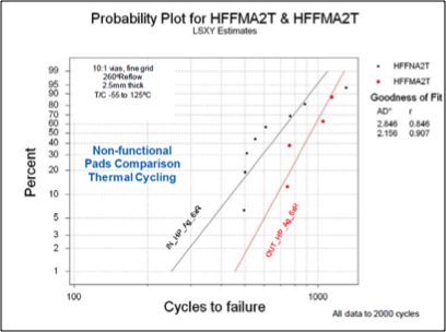
Figure 3. Earlier fails with NFPs.
The paper “Discussion on Nonfunctional Pad Removal / Backdrilling and PCB Reliability”3 indicates that “the continuing trend (which as always is product design specific) is as follows: With smaller vias/higher aspect ratio (0.008"/0.2mm to 0.020"/0.5mm) the inclusion of internal lands is negative (10 to 30% reduction in long-term performance). Conversely, with larger holes/lower aspect ratio (via size 0.020"+/0.5mm+), the inclusion of internal lands is positive (10 to 15% increase in long-term performance).”
In “Design and Construction Affects [sic] on PWB Reliability,” Paul Reid states: “Generally speaking the presence of nonfunctional pads is a determent to the reliability of PWBs.”4 He further points out that one or two nonfunctional pads that are not in the center of the PTH generally improve reliability when compared to the same PTH with NFPs at every layer. He describes a condition call “telegraphing” where there is so much copper at PTHs the material is “resin starved” between pads, and you can see the image of this “pancake stack “of copper in the dielectric; the image is “telegraphed” to the surface. When the dielectric is thin and the copper thick, the condition is exacerbated and reliability is significantly reduced. The high spots create regions where the epoxy is squeezed out. Lack of sufficient epoxy can result in adhesion issues and can provide potential pathways for electrochemical migration to occur. Reid’s schematic is shown in Figure 4. He indicated that is a condition of concern but acknowledged not seeing any real rejections for this condition.
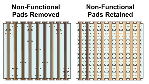
Figure 4. NFP schematic4.
In the book High-speed Circuit Board Integrity,5 Thierauf states that in many situations, NFPs are harmless. However, they can be troublesome in high-speed signaling applications, especially with thick, multilayer boards. Figure 5 shows how an NFP can capacitively couple to a return plane, lowering the impedance seen by a signal passing along the via.
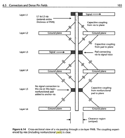
Figure 5. NFP capacitively coupling to plane.
In Chapter 20, “Thermal Stress Issues in Plated-Through-Hole Reliability,” from Thermal Stress and Strain in Microelectronic Packaging,6 the authors refer to industry reports that NFPs are beneficial for PTH life. Modeling with and without NFPs of the Von Mises barrel stress was performed for epoxy glass and Kevlar polyimide multilayer boards (Figure 6).
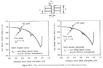
Figure 6. Effect of NFPs on barrel stress.
Industry Expert Opinions
On April 4, 2014, an online Ask the Experts column addressed the topic. A reader asked, “Should we remove nonfunctional pads from inner layers. In some cases, it may be necessary to free up space between rows of pads to route additional trace data. I’ve read articles that favor both options. What is your opinion?” Responses from the experts included:
* “Nonfunctional copper is generally used to balance plating. On innerlayers, with nonfunctional copper, this would be a very sophisticated lay-up, as it sounds as if there are embedded vias and high-density features. With that assumption, replacing nonfunctional copper with functioning copper features is a 1:1 tradeoff. These nonfunctional features are used to “thieve” amperage and/or plating away from sensitive areas. By putting functional copper in these areas, you are balancing the design, to be less dependent on nonfunctional copper.” – Rodney Miller, capital equipment operations manager, Specialty Coating Systems
* “Fabricators normally do prefer it, because it makes drilling easier. Copper is a tough, stringy metal, and in general, it’s a pain to drill through. On the other hand, removal of all unused pads on thick, high layer count PWBs may result in long distances between points where the PTH copper is “tied” into the hole wall. This can result in somewhat reduced reliability. (I’ve seen examples of this.) Selective removal is one option that may provide the routing flexibility needed, and easy fabrication, while maintaining a few tie points along the depth of high-aspect-ratio vias. One approach might be to leave lands on selected plane layers, even if unattached. The plane layers are not used for signal routing, so the presence of pads will not impede routing.” – Fritz Byle, process engineer, Astronautics
* “From a reliability point of view, based on thermal cycle evaluations, removing nonfunctional pads increases the reliability of the PWBs to some degree. It is thought that having nonfunctional pad “in” will cause the drill to work harder as it drills through the extra copper offered by nonfunctional pads and increases the temperature internally, aging the material in the barrel of the hole. Having nonfunctional pad “in” is thought to have a tendency to provide stress risers that focus the strain into the barrel of the PTH. What we find repeatedly is that nonfunctional pad “in” reduces thermal cycle to failure by 10% to 20%. I suggest removing most of the non-functional pads in the central zone of the PWB. Leave in one or two nonfunctional pad in the top or bottom third of the stackup. This will give the most reliable construction. You can always test the two different constructions to prove my contentions, using thermal cycling methods.” – Paul Reid, program coordinator, PWB Interconnect Solutions
* “Nonfunctional pads should be removed if this is a signal via. Nonfunctional pads do not improve reliability from a barrel fatigue perspective and can greatly reduce manufacturability in the drilling process (dulls the drill bit). If the via is used for assembly, such as a through-hole solder joint, then nonfunctional pads can prevent hole wall pull away.” – Dr. Craig D. Hillman, CEO and managing partner, DfR Solutions
* “Eliminating nonfunctional pads is a great way to gain some real estate on all types of PCBs, but this practice should be used with caution on flex and rigid-flex boards. Copper plating generally does not bond to flexible materials in the plated through hole as well as it bonds to rigid materials. This is especially true on controlled impedance flex and rigid flex, where thicker flex dielectrics are incorporated into the material stack up. All pads, both functional and nonfunctional, provide points dispersed along the plated barrel for the plating to adhere to. If all nonfunctional pads are removed, causing the gap between functional pads to become too great, the plating may start to separate from the hole wall. I would recommend leaving at least some of the nonfunctional pads in place on flex and rigid flex boards and attempt to keep them evenly dispersed along the plated through hole wall to avoid possible plating separation.” – Mark Finstad, senior applications engineer, Flexible Circuit Technologies
From these comments, it is clear there is not a “one size fits all” approach to nonfunctional pad removal. Companies need to devise a strategy based on the design and materials used and document those needs clearly to their fabricators. The experts did uniformly recommend removal of NFPs where possible.
Fabricators routinely recommend removal of nonfunctional pads. Multek states that including NFPs adds unnecessary spacing and decreases layer yield,7 illustrated in Figure 7.
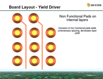
Figure 7. Multek recommendations.
For improved signal integrity at higher frequencies, Sanmina indicates that removal of nonfunctional pads and via backdrilling are two commonly used via optimization techniques.8
Altera offers guidance in at least two application notes.9,10 To minimize parasitic capacitance in high-speed (Gbps) transceiver designs and to optimize vias in high-speed channels in general, eliminating all nonfunctional pads is recommended. Altera further recommends removing NFPs in all high aspect ratio vias.
In “Practical Guidelines for Implementing 5 Gbps in Copper Today, and the Roadmap to 10 Gbps,”11 the authors recommend removal of NFPs, as seen in Figure 8.
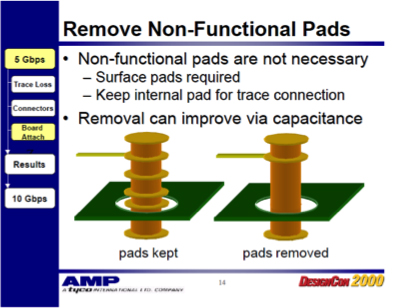
Figure 8. NFP recommendations.
Conclusions
The survey results do not indicate any specific reliability issue associated with the removal of unused pads for standard rigid multilayer boards. Two-thirds of the fabricators who responded removed the pads routinely or after approval from their customer. DfR recommends that designers include this type of acceptance requirement on either their fabrication drawings or their purchase orders.
One supplier for military PBs did indicate that they felt the removal of pads could present a reliability issue. When queried further, it was determined that the issue was with very small drill bits on a 22-plus layer board. In that instance, the additional stiffness from the pads provided support in the drilling operation where the aspect ratio was high.
However, some of the responses and the literature search indicate that the non-removal of unused pads could result in a phenomenon called “telegraphing,” where the epoxy is squeezed so thin that there is a little left between each layer, which can be a reliability issue.4
Acknowledgments
This work was supported by those printed board fabricators who participated in the survey.
This article was first published in the IPC Apex Expo Proceedings, March 2014, and is reprinted here with permission of the authors.
References
1. A. Ciccomancini Scogna, “Signal Integrity Analysis of a 26 Layers Board with Emphasis on the Effect of Nonfunctional Pads,” IEEE EMC Symposium, 2008.
2. Martin Wickham, “Through Hole Reliability for High Aspect Via Holes,” NPL webinar, June 11, 2013.
3. Bill Birch, “Discussion on Nonfunctional Pad Removal/Backdrilling and PCB Reliability,” 2005.
4. Paul Reid, “Design and Construction Effects on PWB Reliability,” IPC Apex Expo February 2012.
5. Stephen Thierauf, High-speed Circuit Board Integrity, Artech House, January 2004.
6. Donald Barker and Abhijit Dasgupta, Thermal Stress and Strain in Microelectronic Packaging, Van Nostrand Reinhold, 1993.
7. Bill Frank, Design for Manufacture, Multek company presentation.
8. Sanmina, PCB Fabrication: Opti-Via Technology for Improved Signal Integrity at Higher Frequencies, company datasheet.
9. Altera AN-672, Transceiver Link Design Guidelines for High-Gbps Data Rate Transmission, company application note, Feb. 15, 2013.
10. Altera AN-529, Via Optimization Techniques for High Speed Channel Design, company application note, May 2008.
11. Brent Rothermal, et al, “Practical Guidelines for Implementing 5 Gbps in Copper Today, and the Roadmap to 10 Gbps,” DesignCon, January 2000.
12. Non Functional Pad Removal. http://wiki.fed.de/images/7/70/Empfehlung_zu_Non_Functional_Pad_Removal.pdf.
GREG CASWELL is marketing director and CHERYL TULKOFF is senior member of the technical staff at DfR Solutions (dfrsolutions.com); This email address is being protected from spambots. You need JavaScript enabled to view it..


