Searching for components and automating schematic capture are just two of the ways AI will be implemented in PCB design.
During the past 10 years, artificial intelligence (AI) has progressed from a visionary concept to a mainstream reality in many large companies. AI is becoming a crucial lever for improving operational productivity and user expertise.
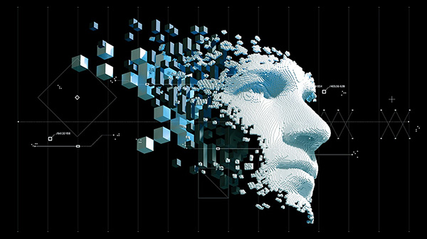
AI is a set of computational technologies that enable a machine to reason and infer without any human intervention. These technologies are developed using cross-disciplinary approaches based on mathematics, computer science, statistics, and psychology. AI based solutions can analyze high volumes of data to identify trends and patterns which can then be used to improve existing processes and make recommendations to assist users in making better decisions.
The world of AI opens a new realm of technologies to propel electronic systems design into the future.
With significant developments in visual and voice recognition, natural language processing, autonomous vehicles, and data mining, AI technologies have become even more advanced and capable of offering enormous advantages toward reducing the complexity of electronic system design and boosting design efficiency, quality and productivity.
Key areas for applying AI for PCB design are those that are largely manual or require expert knowledge of electronic systems design tools. AI enhanced tools empower entry-level users to perform tasks traditionally achievable only by experts.
Expert PCB designers use tools in specific ways to accomplish good design. These users have a deep understanding of the domain and circumnavigate around the nuances of the tools to deliver efficient designs. While it is possible for any engineer to become an expert, it takes years to develop the required skills.
AI mines completed designs for patterns of how tools are used to accomplish a design task and manages that knowledge in a reusable form. This supports better design quality by guiding the designer or engineer to the next logical step without having to search for the step.
Specifically, in the typical electronic systems design process AI technologies – including machine learning and deep learning – can be leveraged in a number of areas to accelerate decision-making, automate mundane processes, improve the efficiency of new users, and optimize the performance and manufacturability of multi-domain systems. These include the following:
Component selection. Design engineers spend a substantial amount of time researching and selecting components that meet the design requirements. They go through datasheets from multiple component manufacturers to find the right set of components that can be used in the design. A model could be developed based on historical information and used to recommend viable options to narrow the search. For example, when a processor is selected, the machine learning model could predict other components needed based on historical knowledge.
Component model creation. Generating models to represent the components (e.g., symbols, 2-D/3-D physical geometries, and simulation models) also takes a substantial amount of time. In large organizations are teams of librarians tasked to go over datasheets of components and convert them into models that can be used in design tools. This not only requires deep electronic domain knowledge but also an understanding of the various tools used to generate models. By using AI technologies, these datasheets can be processed automatically by the system to generate the required models.
Schematic connectivity. Once components are placed in the schematic, establishing the connections is another manual task which is time consuming and error prone. Training a machine learning model by extracting information from a completed design about how components are used and how they are connected enables the schematic capture tool to recommend the components a user might place in the schematic. Once the user confirms the placement, the tool can suggest pin-to-pin connections to speed up the design task.
Dynamic reuse. Functional blocks from completed designs could be analyzed for reuse and managed in an intelligent database that can be searched using various parameters. Training a model with deep learning algorithms to generate a system enables design tools to predict the potential function of a block. Analyzing the components that are placed in the schematic and using the trained machine learning model, schematic design tools can recommend a matching functional block. Similarly, reusable placement and routing blocks can be extracted from completed designs and presented while the designer is laying out a board.
Constraints. PCB designs typically adhere to numerous rules (constraints) for layout, high-speed design, manufacturing and test. This information is usually entered manually into each of the various design tools – a time-consuming and error-prone process. This risk can be considerably managed if the tool can recommend the set of constraints and values that need to be defined for various design objects. These recommendations should be based on the technology used in the current design and knowledge collected from released designs.
Layout – placement and routing. Placement of components and routing of traces take a significant amount of the overall time in a project. Harnessing the knowledge from completed designs, an AI system can recommend placement and routing strategies.
Analysis and verification. Utilizing AI algorithms, analysis and verification tools can generate better designs by understanding various design sensitivities, such as changes in electrical material properties, physical design dimensions and their impact, transceiver I/O characteristics, temperature/voltage variations, and the combined effects of all these variables on the board or system. AI algorithms can be applied to deliver better mesh refinement, to fine-tune user options to produce more accurate simulation results, and to provide better surrogate modeling for via, trace and cable optimizations. Recommending appropriate values for various settings to run various simulations based on historical runs yields better results.
Design synthesis. The ability to auto-generate PCB designs as required and the corresponding manufacturing outputs is the ultimate goal of applying AI to electronic systems design. This not only reduces the time required to complete a design but also eliminates costly mistakes usually caused by manual efforts. Generative design relies on AI algorithms to find an optimal solution through the systematic variation of parameters, structure, or shape of a board. Innovation in AI-driven behavior models for the well-known parts of the board design process speed development of generative design technologies.
By incorporating multi-physics simulation, data analytics, and AI capabilities, EDA vendors' products can demonstrate the impact of design changes, usage scenarios, environmental conditions, and other variables. This will drive down costs, reduce development time, and improve the quality of products and processes.
David Wiens is Xpedition Product Manager in Siemens EDA System Design Division (siemens.com); This email address is being protected from spambots. You need JavaScript enabled to view it.. Over the past 30+ years, he has held various engineering, marketing and management positions within the EDA industry. His focus areas have included advanced packaging, high-speed design, routing technology and integrated systems design. He holds a bachelor's in computer science degree from the University of Kansas.


