Stop thinking such traces must be a certain width!
Au: The general ideas and concepts presented in this paper were first suggested by Nitin Bhagwath in 2017 and presented in a paper at DesignCon in 2018.1
When we start a new board design, we need to meet several objectives. Some of the most obvious are:
- Certain physical constraints must be met (board outline, certain component locations, etc.)
- Point-to-point connection requirements specified in the netlist must be met.
When we start actually routing traces, in broad general terms we work within two paradigms. For now, we will call them “signal” (or i*R), and “power” (or i2*R). The first probably applies to more than 99% of traces. This paradigm relates to how we maintain a clean enough signal so that the system will operate. At a minimum we want to ensure there is not so much voltage drop along the net to cause signal loss and system instability.
We do this by ensuring the resistance of the trace is low enough, and we do that by ensuring the cross-sectional area of the trace is large enough to meet our needs. In the vast majority of cases, the manufacturing limitations are such that the trace is almost always large enough, meeting this requirement inherently. But as systems get more sophisticated, we need to worry about other things:
- Controlling the loop area to control EMI and crosstalk.
- Controlling trace impedance to control reflections.
- Placement of components like bypass caps, and
- Minimizing pad inductance for good power distribution control.
- Dealing with the skin effect and dielectric losses.
Sometimes we even need to worry about via location, impedance and length. As an industry, we now have a lot of information and guidelines regarding how to work within this paradigm.2
Things are a little different when we start dealing with the second paradigm. Here we worry about whether the current level in the trace generates enough power along the trace, and therefore enough heat along the trace, and therefore enough of a rise in temperature, to cause a thermal issue on the board. The power comes from the i2R drop along the trace. Most designers, if working within this paradigm, have one solution: make the cross-sectional area of the trace big enough to lower the resistance low enough to handle the current. And the only place they know to get the answer to how large the trace should be is in the data summarized in IPC-2152.3
This is unfortunate. As Brooks and Adam have shown,4 the IPC data are almost always worst case. That is, almost anything we do to a trace from a practical standpoint lowers the temperature of the trace. This area is very complex, and it is very hard to make generalizations because almost all examples are case-specific. But in the examples Brooks and Adam look at in their book5:
- Reducing the length of a trace can lower the change in temperature by perhaps 20%.
- Adding a parallel trace can lower the change in temperature by perhaps 14%.
- Placing a plane on the opposite side of the board can lower the change in temperature by perhaps 30%.
- And placing a plane on the layer directly under the trace can lower the change in temperature by up to 50%.
As a result, many designers use larger traces than required, using up valuable real estate. But the examples above only touch a fraction of the opportunities that might be available to designers. In this article we will suggest that thinking outside the box may allow many designers to achieve their thermal objectives much more efficiently than ever before. We may be able to add non-current-carrying copper areas and trace segments, not for signal reasons, but for thermal reasons.
Caution: Some designers, in initial discussions about this topic, immediately dismiss the concepts presented herein as being impractical because a) the designers think they don’t have enough real estate on the board to implement them, or b) they think the ideas are inconsistent with their perceived signal integrity needs. This is a mistake! It is very rare for the same trace to be subject to both paradigms (signal and thermal) suggested above at the same time. And thermal issues can often be confined to areas of a board where real estate requirements can be a little more flexible.
A trace heats by i2R. The primary cooling mechanism for a trace is conduction (heat spreading) into and through the board material (dielectric) before heat ejection from the board through convection and radiation. Anything that increases the efficiency of the thermal conduction lowers the temperature. That is why, for two traces with the same cross-sectional area carrying the same current, the thinner, wider trace will have a lower temperature. That is why a copper plane directly under the trace lowers the trace temperature.
What we are advocating here is that, first of all, designers stop thinking about high-current-carrying traces as being a certain width. We tend to look at the IPC-2152 tables and think, “Okay, my trace needs to be x mils wide.” No, it can vary in width. And if we vary the width, then the wider sections can draw heat away from the narrower sections. Second, we advocate that designers consider various ways to add copper surface area to their designs in such a way as to conduct heat away from traces. Adding a plane under the trace is one obvious way to do that. There may be other ways we can approach this.
In the rest of this article, we will offer suggestions of ways to think about these options. But, there is an infinite number of ways we can do this. Every example here can be implemented any number of ways, with any number of shapes and dimensions. There is no one answer. In fact, it is really hard to even make generalizations, although we will try to offer some insights. At the end of the article we will offer suggestions on how a designer can proceed.
Test Board
In the examples below, we will assume a standard test board 220mm long by 20mm wide (8.7" x 0.8"). Its thickness will be 1.55mm (approx. 61 mils), including 38µm (1.0 oz.) trace layers top and bottom. A stackup is provided in FIGURE 1. The standard (reference) trace on the board’s top layer will be approximately 150mm (6.0") long by 1.0mm (40 mils) wide. The board dielectric material will be polyimide. We will apply 4A of current through the trace. We will simulate our examples and calculate temperatures using a simulation program called Thermal Risk Management (TRM).6 The temperature of the simple trace, with no adjacent traces or planes and with no supplemental cooling, rose from an ambient of 20oC to 53.2oC, or a change of 33.2oC.
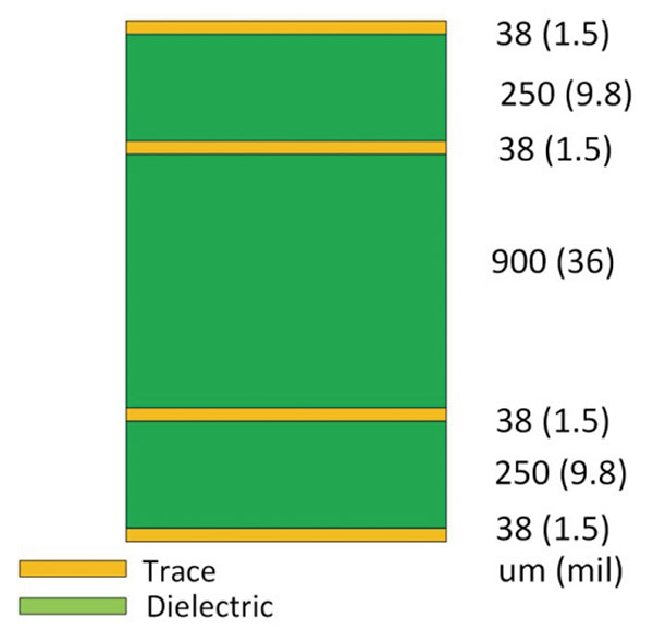
Figure 1. Stackup of test board (not to scale).
Example 1: Copper under the trace. Adding copper under the trace will help conduct heat away from the trace, lowering the trace temperature. We looked at five configurations, summarized in TABLE 1 and in FIGURE 2. These included:
- The trace with no supplemental cooling.
- Placing a trace the same width on the trace layer under the trace.
- Placing a trace three times wider than the trace (120 mils) on the trace layer under the trace.
- Placing a full copper plane on the bottom trace layer.
- Placing a full plane on the trace layer under the trace.
Table 1. Basic Data
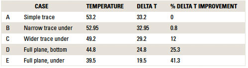
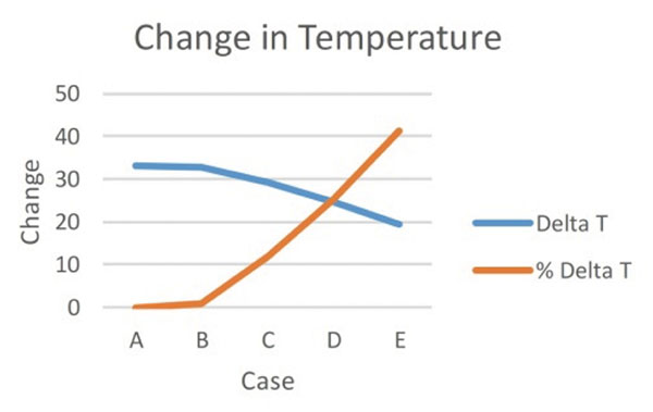
Figure 2. Change in temperature data from Table 1.
Discussion. Two conclusions are intuitive. The more copper we can place under a trace, the more heat is conducted away from the trace, and the cooler the trace temperature will be. The closer the copper is to the trace, the more heat is conducted away from the trace, and the cooler the trace temperature will be. The more heat that is conducted away from the trace, the smaller the trace can be and still carry the target amount of current. So, look for ways to add copper underneath the trace.
It should be noted a copper area used specifically for cooling carries no current whatsoever. And even if there is some small amount of noise signal coupled to it from the power trace, that coupled current should be harmless. If there is any concern at all about a coupled current, simply tie the copper area to the system reference (ground) with a single via.
From a thermal standpoint, any underlying plane works like any other plane. The underlying plane does not have to be a “continuous and related” plane in the sense we need that for the signal paradigm (signal integrity.) However, a systems engineer needs to determine whether any noise on the high-current-carrying trace might couple into any underlying, unrelated (and sensitive) plane.
Adding vias (i.e., “thermal” via) connecting traces to planes in any of these configurations resulted in trivial (if any) improvement. As we have shown in our book, traces can cool vias, but not the other way around. Vias do not cool traces.7 On the other hand, any vias that might be penetrating the planes from other nets are inconsequential. They have a minimal impact on the cooling area of the total plane.
Example 2: Adding additional copper to traces. It is not necessary for a high-current-carrying trace to be constant width. There may be opportunities to change the width as the trace routes across the board. For this example we added nine “stubs” or pads, equally spaced along the trace. The stubs increased the width of the trace from 1.0mm to 5.0mm at each point. They were spaced 15mm apart. FIGURE 3 is an illustration from the simulation output showing the configuration.
Figure 3. Trace with distributed “stubs” along its length.
With just a simple trace, the maximum trace temperature was 53.2oC. Adding the distributed stubs lowered the peak temperature to 44.4oC. The corresponding changes in temperature were 33.2oC and 24.4oC, respectively, an improvement of 26.5%. This means we could, for example, decrease the width of the standard trace without exceeding our maximum allowable trace temperature. The thermal profiles of the two cases are shown in FIGURE 4.
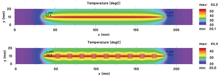
Figure 4. Thermal profiles showing the simple trace and a trace with numerous stubs along its length.
Discussion. If we do not constrain ourselves thinking that high-current-carrying traces should be a constant width, we open up all kinds of opportunities to change the width to help conduct away heat. So if, for example, we calculate a trace 40 mils wide is needed to carry the current, we may be able to reduce that width in some areas of the board, while increasing it in others without increasing the maximum tolerable trace temperature.
The largest part of the current is carried along the line of the trace. There is a little current fringing into the stub, but not very much. FIGURE 5 shows the current density along a portion of the trace.
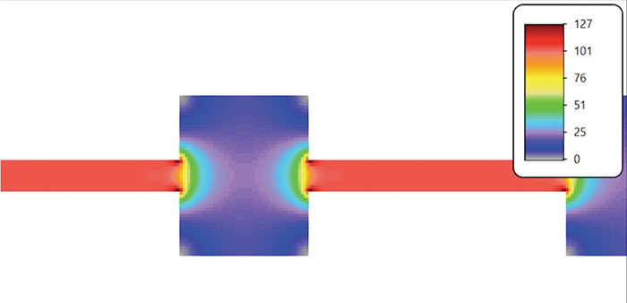
Figure 5. Current density along trace (units are A/mm2).
Example 3: Dealing with connecting links. In a recent article, we discussed how short, narrow connecting links along high-current-carrying traces are not as troublesome as some might think.8 The main trace acts as a heatsink for the link, conducting a significant part of the heat away from the link, helping to lower the temperature of the link. In this example we will look at three link configurations (FIGURE 6):
- A single, short, 3-mils long, 11-mils wide connecting link between two sections of the test trace. Such a link may be required if we have to bring the primary trace near some components that restrict the area around the trace. This link looks a lot like a fuse!
- The addition of a second link using a nearby path.
- The addition of a small, supplemental area of copper (partial plane) directly underneath a single link. This copper area is 40mm long by 6mm wide (1.6" x 0.25").
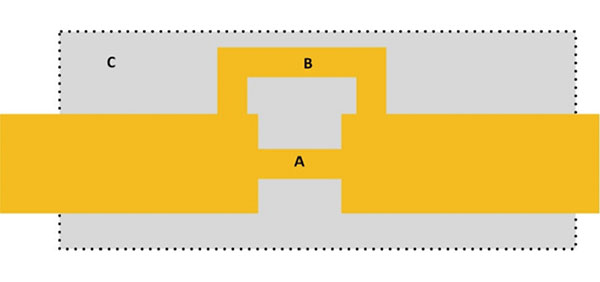
Figure 6. Three link configurations (not to scale).
The results of these simulations are shown in TABLE 2. A single, 11-mils wide trace, by itself, carrying 4.0A would heat to well over 150oC. But because of the heat-sinking influence of the basic trace, the trace temperature doesn’t rise nearly that much. But it does increase, perhaps to intolerable levels. If we put a small plane under it, the temperature only increases about 13%. Adding a parallel second link, the benefit is about the same as adding an underlying plane. The thermal profiles of the three cases are shown in FIGURE 7.
Table 2. Example 3 Data
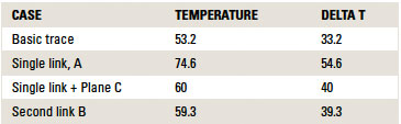
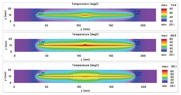
Figure 7. Thermal profiles of the three cases.
Discussion. If we are constrained in our thinking that high-current-carrying traces must be a certain width, and then we run into a constricted area on the board, it would seem we had few, if any, options. But if we relax that restriction, several opportunities may present themselves. It certainly may be possible that a second (albeit narrow) adjacent path (or even more) might be available. This would allow spreading out the heat-generating area of the trace over a wider area, helping to control the trace temperature.
The “plane” area under the link area doesn’t necessarily need to be continuous. In fact, it need not even be a single area. There might be an opportunity to spread copper around the layer between other traces. And any via paths that might exist through the “plane” are almost inconsequential as far as the heat-spreading ability of the copper is concerned.
Conclusions
When we start worrying about signal integrity issues in PCB design, we start worrying about rules: loop area must be minimized; trace impedance must be constant; pad impedance must be minimized, etc. We are now advocating that when designing high-current-carrying traces we forget the rules (i.e., the trace must be a minimum size). Instead, start thinking outside the box. Think how can I lower the trace temperature in ways other than just increasing its cross-sectional area? As a start, we can add (non-current-carrying) copper areas near and under the trace to help conduct heat away. We can design traces with wider widths where there’s room and narrower widths where there’s not. The wider areas will help sink some of the heat away from the narrower areas. In this way we will achieve much more flexibility in our layouts, especially in tight areas.
How to evaluate design alternatives. The good news from all this is there may be some really significant options available if we look. The bad news is it is really difficult to evaluate them! In the mid ‘90s our industry first began looking at controlled impedance traces in a significant number of designs. We needed to know how to calculate trace impedance and how to calculate trace parameters to meet a target impedance. Back then we had formulas published by various trade associations and manufacturers. Today we know these formulas are not accurate enough. We now say we need “field effect” solutions to meet our requirements, computer programs that use matrix algebra to solve a large number of simultaneous equations, resulting in the solutions we need.
When it comes to thermal design, we have relied on the charts published by IPC for a long time. But the problem is much more complicated than simply adding the thermal resistance and local heating of individual traces. We now need the same types of computer programs as needed for impedance: programs that use matrix algebra to solve a large number of simultaneous equations, resulting in the solutions we need. The equations are different, but the process is the same. In general, this category of program is called “thermal simulation.” And as systems get more complex, we will need these programs at both the board level and the systems level.
Notes
- Nitin Bhagwath, Doug Brooks, Robin Bornoff, Praveen Anmula, Joseph Aday, Robert Carter, and Patrick Carrier, “Non-Conventional Approaches for Maximizing Current Capacity of a PDN,” DesignCon, January 2018.
- Douglas G. Brooks, Ph.D., PCB Currents; How They Flow, How They React, Prentice Hall, 2017.
- IPC-2152, “Standard for Determining Current Carrying Capacity in Printed Board Design,” August, 2009, IPC. This is an update of the charts that appeared in IPC-2221, which themselves traced back to National Bureau of Standards Report #4283, published in 1956.
- Douglas G. Brooks, Ph.D., and Dr. Johannes Adam, PCB Trace and Via Temperatures: The Complete Analysis, 2nd Edition. See also Johannes Adam’s earlier paper, “New Correlations Between Electrical Current and Temperature Rise in PCB Traces,” Proc. 20th IEEE SEMI-THERM Symposium, 2004.
- Brooks and Adam, Section 6.3 and especially Table 6.5, p. 70.
- TRM (Thermal Risk Management) is designed to analyze temperatures across a circuit board, taking into consideration the complete trace layout with optional Joule heating, as well as various components and their own contributions to heat generation. Learn more about TRM at www.adam-research.com. Examples of how to use TRM are in Brooks and Adam, Chapter 6.
- Brooks and Adam, Chapters 7 and 8.
- Douglas Brooks, Ph.D. and Dr. Johannes Adam, “More on Via Temperatures,” PCD&F, June 2018.
Douglas Brooks, Ph.D., is president of UltraCAD Design, a PCB design service bureau and author of three books, including PCB Trace and Via Currents and Temperatures: The Complete Analysis, 2nd edition (with Johannes Adam) and PCB Currents: How They Flow, How They React; This email address is being protected from spambots. You need JavaScript enabled to view it.. Nitin Bhagwath is a product architect at Mentor (mentor.com); This email address is being protected from spambots. You need JavaScript enabled to view it..


