A new calculator for measuring delay and capacitance per unit length and characteristic impedance.
One of today’s primary challenges of the technological progress is the development of the scientific foundations for further improvement of the elements and structures of the computer technology. The areas of research targeted at boosting performance of the computing devices include such issues as the improvement of the design of the multilayer printed circuit boards (MLB) as the main structural and contact elements in modern computing systems. Some issues are at the forefront of research, such as an efficient simulation of the MLB communication lines and the development of hardware and software that are used to put the simulation results into practice.
Despite intensive research on various aspects of problems related to multilayer printed circuit board (MLB) communication line simulation, some open scientific tasks in the spheres of development and improvement of computing elements and devices still exist.1,2 Such issues are associated with analysis and synthesis of the MLB communication lines for high-performance computing systems for the subnanosecond time range, including special switched meander delay line structures, as well as development of software applications to support new pre-design simulation techniques for multilayer PCBs with the flexible topology of communication lines.1,2
This article addresses issues related to the development and organization of production of hardware and software tools for debugging microprocessor systems and programs, which are a part of the hardware-software complex. Each type of communication line has an individual set of design electrical parameters from a common set of parameters that determines the quality (integrity) of pulse signals during the exchange of information in printed transmission lines. The key parameters to be measured are the extrinsic electrical parameters of the communication lines.3,4
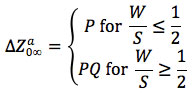
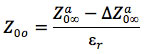
The extrinsic electrical parameters of the communication lines are as follows:
- The characteristic impedance of a single transmission line at high frequencies – Z0. This parameter is used to determine the level and shape of the reflection noise;
- The differential characteristic impedance of the coupled lines at counter currents – Z0 diff. This parameter is used to determine the rating of the terminating resistor during the push-pull transmission of the data signals (LVDS);
- The transmission line delay constant at high frequencies – Т0. This parameter is used to measure the delay of distortionless pulses by the base;
- The attenuation coefficient of a harmonic signal at the frequency f-α0R. This parameter is required to calculate a signal rise roll-off in the long lines (skin-effect);
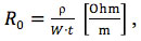
- Resistance per unit length of a signal line at the direct current – R0. This parameter is required to calculate the steady-state value of a transient process.
FIGURE 1 shows the design of a printed circuit board with the meander communication lines.
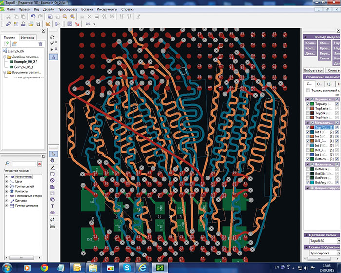
Figure 1. Structure of a PCB with meander delay lines.
The scheme given in FIGURE 2 illustrates the examples of data input for processing in the XML format (the eXtensible Markup Language describes a document and partially describes the behavior of computer programs) individually for the microstrip transmission lines with consideration for the topology of a microstrip line. The microstrip line topology is shown in FIGURE 3
where
W = the signal strip width;
h = height of a rise of a printed track over the support layer;
t = thickness of the conductive layer;
εr = the relative permittivity of a substrate.
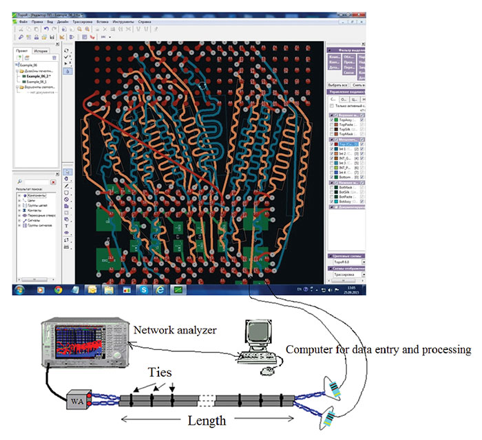
Figure 2. Wiring diagram of a network analyzer (calculator) to measure the communication line parameters (WA – wave adapter).
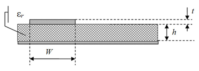
Figure 3. The microstrip line topology.
The design electrical parameters of a microstrip line are as follows:
- The characteristic impedance of a transmission line at high frequencies – Z0. This parameter is required to calculate the reflection noises;
- The inherent delay of a transmission line at high frequencies – Т0. This parameter is required to measure the delay in a distortionless communication line;
- The attenuation coefficient of a harmonic signal at the frequency f-α0R. This parameter is required to determine the shape of a pulse rise roll-off at the end of a terminated communication line;
- Resistance per unit length of a signal line at the direct current – R0. This parameter is required to calculate the steady-state level of voltage at the end of a parallel terminated communication line.
Steps for calculating the characteristic impedance of a microstrip structure:
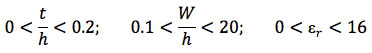
- Checking the working range of design formulas for Z0:
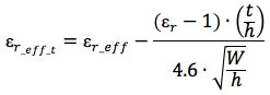
- Calculation of the effective relative permittivity (an auxiliary parameter):
- a narrow printed track (W < h):
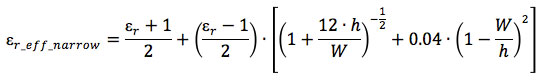
- a wide printed track (W ≥ h):
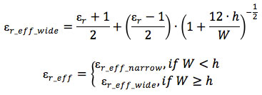
- allowance for the track thickness t:
- Calculation of the effective width of a printed track (an auxiliary parameter):
- a narrow printed track (2πW < h):
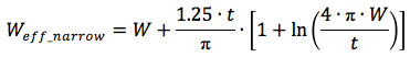
- a wide printed track (2πW ≥ h):
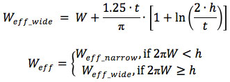
- Calculation of the characteristic impedance:
- a narrow printed track (W < h):
 (Eq. 1)
- a wide printed track (W ≥ h):
 (Eq. 2)
 (Eq. 3)
The Z0 calculation error in the working range is not greater than 2%.
Comparison of calculations made using the calculator with those made using HyperLynx is shown in FIGURE 4.
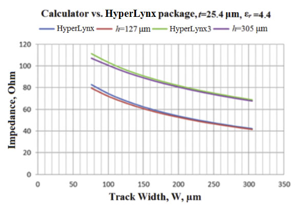
Figure 4. Comparison of calculated values using the calculator vs. HyperLynx.
- Calculation of the delay per unit length of a microstrip lin
 (Eq. 4)
- Calculation of the attenuation coefficient. The attenuation coefficient of a microstrip line due to metal conductor losses at the frequency f [GHz]
 (Eq. 5)
where  - specific resistivity of the conductive material.
For copper ρ = 0.0176 [Ohm·mm2/m],
- Calculation of the resistance per unit length of a signal line at the direct current:
 (Eq. 6)
where  – the specific resistance of the centered track.
For copper ρ = 0.0176 Ohm·mm2/m
- Calculation of the capacitance per unit length:
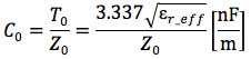
- Calculation of the inductance per unit length:
- Calculation of the signal strip width (W) at a given differential characteristic impedance (Z0) (the Synthesis Mode).
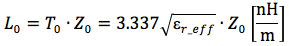
The geometry of a microstrip line in a dielectric medium is shown in FIGURE 5.
Figure 5. The geometry of a microstrip line in a dielectric.
W = the signal strip width;
h1 = the height of a rise of the dielectric over the signal strip;
h2 = the height of a rise of the printed track over the lower backup layer;
t = thickness of the conductive layer;
εr = specific relative permittivity of the substrate.
The design electrical parameters of a microstrip line:
- the characteristic impedance of a transmission line at high frequencies – Z0;
- the inherent delay of a transmission line at high frequencies – Т0;
- the harmonic signal attenuation coefficient at the frequency f – α0;
- resistance per unit length of a signal line at the direct current – R0.
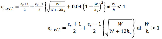
Steps for calculating the characteristic impedance of a microstrip structure in a dielectric medium:
- Calculation of the characteristic impedance of a line at the surface of a dielectric medium (an auxiliary parameter):
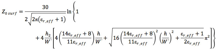
- Calculation of the effective width of a signal line (an auxiliary parameter):
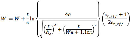
- Calculation of the effective relative permittivity of a microstrip line (an auxiliary parameter):
- Calculation of the characteristic impedance of a microstrip line embedded in a dielectric medium:
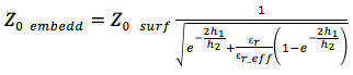 (Eq. 7)
FIGURE 6 shows a comparison of the calculated values obtained using the calculator with those obtained using HyperLynx.
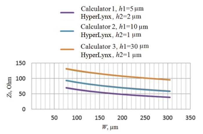
Figure 6. Comparison of calculated values using the calculator vs. HyperLynx for a microstrip structure in a dielectric medium.
- Calculation of the delay per unit length of a microstrip line:
- Calculation of the resistance per unit length of a signal line at the direct current – R0:
 – resistance of a printed strip at the direct current,
where  – the specific resistance of the
centered printed track. For copper ρ = 0.0176 Ohm·mm2/m.
Differential Microstrip Line
The topology of a differential microstrip line in a dielectric medium is shown in FIGURE 7.
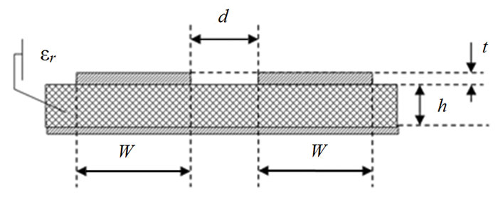
Figure 7. Differential microstrip line topology.
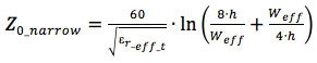
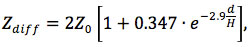
- Calculating the differential characteristic impedance of a microstrip structure is as follows:
- Calculation of the differential characteristic impedance at the given d and W:
 (Eq. 8)
where Z0 smsl = the characteristic impedance of a single microstrip line (Equations 1, 2 & 3).
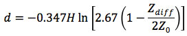
- Calculation of a distance between the adjacent lines (d) at a given differential characteristic impedance (the Synthesis Mode):
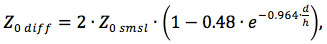
Calculation of the signal strip width (W) at a given differential characteristic impedance (Z0 diff) and a given distance between the coupled lines (the Synthesis Mode).
The width of a strip is calculated by using an iterative method (FIGURE 8).
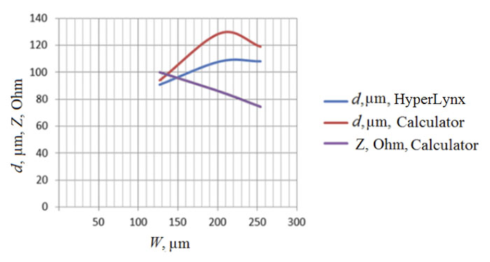
Figure 8. Comparison of calculated values using the calculator vs. HyperLynx for a differential microstrip structure.
Symmetrical Strip Line (h1 = h2)
The geometry of a microstrip line in a dielectric medium is shown in FIGURE 9
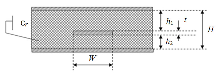
Figure 9. Strip line geometry (h1 = h2).
where
W = the signal strip width;
h1 = the height of a rise of the printed track over the upper support layer;
h2 = the height of a rise of the printed track over the lower backup layer;
t = thickness of the conductive layer;
εr = specific relative permittivity of the substrate.
H = h1+h2+t – distance between the support planes.
The design electrical parameters of a stripline are as follows:
- The characteristic impedance of a transmission line at high frequencies – Z0;
- The inherent delay of a transmission line at high frequencies – Т0;
- The harmonic signal attenuation coefficient at the frequency f – α0;
- Resistance per unit length of a signal line at the direct current – R0.
Steps for calculating the characteristic impedance of a symmetrical strip structure (h1=h2=h):
- Calculation of Z0 narrow– a narrow printed track (W ⁄ H) < 0.35:
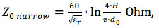 (Eq. 9)
where
d0 = the diameter of a circular cross-section conductor, which is equivalent to a rectangular strip:
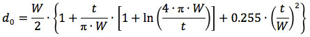
- Calculation of Z0 wide, – a wide printed track (W ⁄ H) > 0.35:
 (Eq. 10)
where
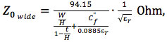
 = an edge capacitance [pF/cm] between one edge of a strip and the adjacent grounded plane:
- Calculation of the delay per unit length of a microstrip line:
- Calculation of the attenuation coefficient in copper of the conductors (skin-effect) for a narrow track case – W/(H–t)<0.35 and t/H<0.25:
 (Eq. 11)
From here on, the surface resistance of copper Rf is equal to:
Rf = 8.25 * 10-3√f , Ohm/m2, where f – frequency, GHz
- Calculation of the attenuation coefficient in copper of the conductors (skin-effect) for a wide track case – W/(H–t)>0.35:
 (Eq. 12)
The Z0 calculation error in the working range is no greater than 1.5%.
The comparison of Z0 calculations using the calculator with those using HyperLynx for a symmetrical strip line is shown in FIGURE 10.
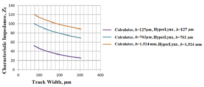
Figure 10. Comparison of calculated values using the calculator vs. HyperLynx.
- Calculation of the delay per unit length of a microstrip line:
 (Eq. 13)
- Calculation of the resistance per unit length of a signal line at the direct current – R0:
– resistance of a PCB strip at the direct current,
where  – the specific resistance of the central printed track. For copper ρ= 0.0176 Ohm·mm2/m.
The calculated values obtained using the calculator are practically in close agreement with those obtained using HyperLinx at h – the height of a strip line (Figure 10).
Asymmetrical Strip Line (h1≠ h2)
The characteristic impedance of an asymmetrical strip line is calculated as a parallel connection of two characteristic impedances of the symmetrical strip structures (Eq. 9, 10) having a different distance between the reference planes H1=2h1 и H2=2h2:
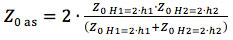 (Eq. 14)
Differential Stripline on the Narrow Side of a Conductor
The geometry of a differential microstrip line in a dielectric medium is shown in FIGURE 11.
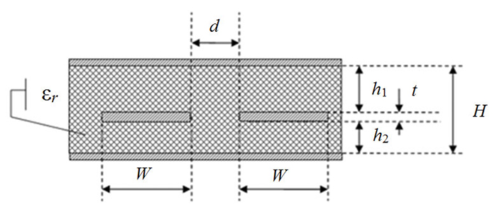
Figure 11. Geometry of a differential stripline on the narrow side of a conductor.
Steps for calculating the differential characteristic impedance of a strip structure on the narrow side of a conductor:
- Calculation of the differential characteristic impedance of a microstrip structure on the narrow side (Analysis Mode and Synthesis Mode):
where
Z0 – the characteristic impedance of a single stripline (Eq. 9, 10, 14)
- Calculation of a distance between the adjacent lines (d) at a given differential characteristic impedance Zdiff (the Synthesis Mode)
- The width of a strip is calculated by using an iterative method as shown in Figure 11 (the Synthesis Mode).
Differential Symmetrical Stripline on the Wide Side of a Conductor (Analysis Mode and Synthesis Mode)
The geometry of a differential microstrip line on the wide side of a conductor is shown in FIGURE 12.
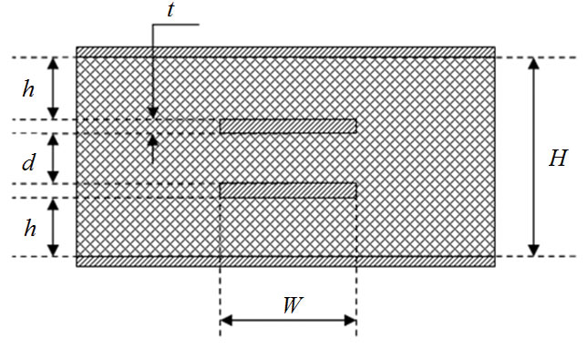
Figure 12. Geometry of a differential stripline on a wide side of a conductor.
Steps for calculating the differential characteristic impedance of a strip structure on the wide side (the Analysis Mode):
- The intermediate calculated parameters are:
- The characteristic impedance of a single line with the intermediate parameters is:
- The intermediate parameter Р is:
- The intermediate parameter Q is:
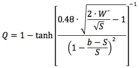
- An increment of the characteristic impedance of a single line with the intermediate parameters is:
- The resultant characteristic impedance of a single stripline with a symmetrical strip is:
- The differential characteristic impedance of the lines coupled on the wide side is:
Zdiff = 2 * Z0o
- The Synthesis mode. A distance between the symmetrical strips d for a given characteristic impedance is calculated using the Synthesis algorithm.
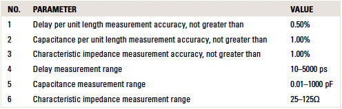
The primary function of the measuring device calculator is to perform a quick measurement of the delay per unit length, capacitance per unit length and characteristic impedance of the printed test-transmission lines on the MLB in mass production.
The calculator functions as a self-contained measuring device, and is capable of measuring the delay per unit length, capacitance per unit length and characteristic impedance of the printed test transmission lines of the multilayer PCBs. The major expected parameters of the characteristic impedance measuring device are in TABLE 1.
Table 1. The Basic Parameters of the Characteristic Impedance Meter
The proposed methods, algorithms and equations, as well as the comparative evaluation of the calculator methods, suggest this domestic device is capable of measuring the key parameters of the communication lines in high-speed computing systems. Compared to the import devices of the same type known in Russia, the calculator has certain advantages and can be used when designing the domestic computing systems.
References
1. S.A. Sorokin, Theoretical and Methodological Fundamentals of the Printed Circuit Board Design for High Performance Computer Applications, Moscow, MIREA, 2017.
2. A.V. Parfenov and S.M. Chudinov, “Trends in the Development of Computer Technologies,” Nauchnye Vedomosty BelSU, no. 16 (237), issue 39, 2016.
3. D.M. Malinichev, S.A. Sorokin and S.M. Chudinov, “Research and Selection of the PCB Transmission Line Parameters for Computer Systems,” Voprosy Radioelektroniki, OT series, vol. 11, 2015.
4. D.M. Malinichev, S.A. Sorokin and S.M. Chudinov, “Selection of Cross Section for the Transmission Lines in Computers,” Voprosy Radioelektroniki, OT series, vol. 11, 2015.
5. A.A. Amosov, Yu.A. Dubinsky and N.P. Kopchenova, “Computational Techniques for Engineers,” Vysshaya Shkola, 1994, ISBN 5-06-000625-5.
Stanislav M. Chudinov, Ph.D. is professor and scientific adviser to the general director of NIIVK (Scientific Research Institute of Computer Systems); This email address is being protected from spambots. You need JavaScript enabled to view it.. Sergey A. Sorokin, Ph.D., is chief designer of NIIVK; This email address is being protected from spambots. You need JavaScript enabled to view it.; and Aleksey P. Sorokin is a post-graduate student of NIIVK; This email address is being protected from spambots. You need JavaScript enabled to view it..


