Test results for two new scientific methods for modeling striplines on high-performance devices.
Computer system designers currently use a host of international standards, GOST 21552-84 Computer Equipment, International Electrotechnical Commission (IEC) publications, as well as their own guidelines for developing specific types of computer equipment employed for the analysis and synthesis of transmission line parameter control.
The authors optimized electrical and design parameters of transmission lines used in computer systems developed by the Research Institute of Computing Systems.1 Here, an approach is described for using the simulation tools to improve data exchange reliability through the use of the transmission lines, including on multilayer printed circuit boards.2,3
Synthesis of the electrical and design parameters. Synthesis is always considered to be basic to the theory of control. Here, the authors provide information on synthesis of the electric and design parameters of the transmission lines for third- and fourth-generation computer systems.
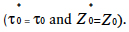
The uniform transmission lines of computers are characterized by the length l; the reactive parameters per unit length, capacitance C0 and inductance L0 (also called the lumped parameters); or the wave parameters, characteristic impedance Z0 and propagation delay per unit length τ0. Besides, their properties are the losses per unit length: the resistance R0 of a wire and dielectric conductance G0.
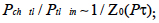
A unique relationship exists between lumped and wave parameters

Dielectric conductance can be neglected in the transmission lines between the logic elements of a computer. Let’s assume G0 = 0.
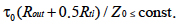
Propagation time (τtl) for a signal passing through a transmission line is determined by its length, delay per unit length, loss resistance, signal source output resistance (Rout) and line connection mode. The minimum signal transmission time is typical for a line with a low-loss resistance (Rtl = R0l << Z0), which is match terminated (τtl = τ0l). Such a line connection mode is usually used in connections between chips (ICs).
For mismatched lines without any losses at Rout ≥ Z0 the signal propagation time will be
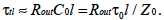
If there are losses (Rtl ≥ 2Z0), and with a low output resistance, the signal propagation time can be calculated as follows:
Generally, the following equation can be used for the approximate evaluation of signal propagation time for the mismatched lines
 (Eq. 1)
within the range of  Such line connection mode is normally used for connections inside the chips. In this case, an increase of
  compared to τ0l is mainly due to an increased propagated signal rise time. However, the rise time should not exceed an inlet gate actuation time
  The instability of actuation time would otherwise be excessive, or there might be a false actuation of the receiver. Thus, the following condition has to be met for the longest lines

where k is the coefficient.
For the specified elements and lmax determined by the chip size, the condition (Eq. 1) may be written as
 (Eq. 2)
The analysis of equations for signal propagation time at different connection line modes and the conditions (Eq. 2) clearly show the need to reduce the delay per unit length. This is an unconditional requirement, and it does not depend on the other parameters.
However,  is proportional to
  (the relative dielectric permittivity). Thus, a technological challenge is to minimize the dielectric permittivity of the medium where the transmission lines are laid out. Silicon oxide with
  is usually used for the chips, while today’s materials for multilayer printed circuit boards have
  We expect that in the future,
  of backplanes will be further reduced.
Three main factors determine the right choice of another basic line parameter: characteristic impedance; line nonuniformity caused by the taps from these lines to the intermediate receivers; power consumption during transmission of the signals over the transmission lines; and line cross-section geometrical parameters, which restrict the line density in routing space.
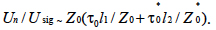
The taps from the mainline to the intermediate receivers distort the uniformity of the line and cause reflection noise Un. For an amplitude of the desired signal Usig>>Un under the real condition, a tap can be represented as the equivalent capacitance Ctap and Un/Usig ~ Z0Ctap, where Z0 = the characteristic impedance of the mainline. Generally, a tap comprises several consecutive line segments located in various routing spaces, and they have different parameters. FIGURE 1 illustrates a tap consisting of two segments: The first one has the length  and it has the parameters of the mainline, and the second segment
  in length has
  and
and  ; at the end, the tap is loaded by an input capacitance
  (p-n-junction capacitance).
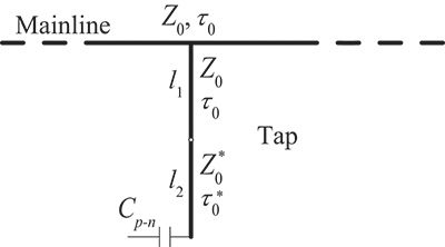
Figure 1. Scheme of a line tap to an intermediate receiver.
The capacitance of the tap can be expressed as the sum of capacitances:
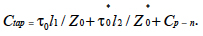
Typically,  is very small compared with the other components, and it can be neglected. Thus,
 (Eq. 3)
If a connection is located entirely in one routing space, i.e. in a chip, the wave parameters of the tap segments will be similar:
Eq. 3 will be as follows: 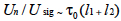 . This suggests that in this case, the noise level does not therefore depend on the characteristic impedance of the line.
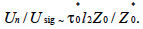
If a connection is located in various routing spaces:  in a backplane,
  in a chip, the wave parameters of the tap segments might be different. For the high-speed elements where it is important to have
  Eq. 3 is then converted to
If the design of a chip is predetermined, i.e., the value of  is predetermined, the noise level will be less than
  – the characteristic impedance of the lines on a backplane. When using packaged chips (IC chips), the length
  will be significant. The lines on a backplane should have a low characteristic impedance in order to minimize the reflection noise level. However, when the chips and backplanes are implemented with a balanced design, we can assume
  (the equality constraint), in which case the characteristic impedance will have no effect on the reflection noise level. Moreover, taking into account the recent trend toward the use of bare chips, the length
  can be substantially reduced, especially when the line inputs to a chip are located not along its perimeter, but along the chip base in the immediate vicinity of the receiving elements. Thus, there exist the real prerequisites for reducing the reflection noises from the line taps and making their value independent of the characteristic impedance of the transmission lines.
The own power input of the chip elements without considering their actions in the transmission line is:
 (Eq. 4)
No forced matching is needed for the transmission lines made entirely in a chip. Taking into consideration the said assumption that each gate (i.e., each connector circuit) switches over once during the clock cycle, we can determine, at least, without regard to power in loss resistance of the lines, the power required to transmit signals through the transmission lines of a chip is

where
Cch = the total capacitance of the chip transmission lines
kp = coefficient for power dissipation in the gates when transmission lines are connected to them.
As for the wave parameters, we have the following

where
 = the total length of lines in a chip.
According to Kolesnikov et al,2

where
А = a side of the chip (assuming a chip is square-shaped). Finally, we have
 (Eq. 5)
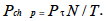
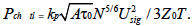
Typically, the transmission lines on a backplane between the chips are match-terminated, and they consume the static power. Given the gate conditions “1” and “0” are equally likely on the average, we can find the value of the power for one matched circuit: 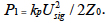 The power required to match the board circuits per one chip on the average is
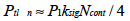
where
Ncont = the number of external chip contacts
Ncont / 4 = the number of external output contacts
ksig = the coefficient that indicates what part of the circuits needs to be matched.
For the functionally incomplete chips – 
We finally have
 (Eq. 6)
Let’s find the per unit values for the power components:
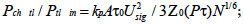

With the advance of microelectronics and reduction of Pτ parameter, the N value increases proportionally to  for the optimal speed gates. Also taking into account the values of kp, ksig, A and Usig vary slightly, partially compensating each other, we can roughly get the following from Eq. 4 to Eq. 6:
 (Eq. 7)
 (Eq. 8)
Eq. 7 and 8 clearly demonstrate that when further developing the microelectronics, i.e., decreasing the value of  , a portion of power used to transmit the signals over the transmission lines increases almost linearly. The radical method for reducing the power is to increase the characteristic impedance of the lines.
The cross-section of the transmission lines in multilayer routing structures (FIGURE 2) can be characterized by the following geometric parameters: the width and thickness of a signal line strip – W and t, respectively, dielectric thickness H with the specific permittivity ε, and signal line spacing b within a single layer. The different technologies might have different restrictions on a multilayer structure. There may be restrictions on the total thickness of the structure, which is typical for the multilayer PCBs, or there may be restrictions on the number of layers of the structure, which is common for the chips. In the first case, the maximum achievable density of transmission lines corresponds to the minimum value of bH, and in the second case, the minimum value of b. The only argument of the function is the characteristic impedance of the lines.
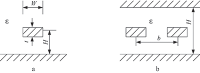
Figure 2. Stripline cross-section: а – open, b – closed.
When implementing the optimization results using the simple models that require a small memory capacity and provide an estimate of delays per unit length based on the aforementioned analytical equations, the result with an average error of no more than 5% can be obtained.
References
1. S.A. Sorokin and S.M. Chudinov, “Current Issues in Modeling the Printed Conductors of Multilayer Printed Circuit Boards when Developing the Domestic CAD System,” Radiopromyshlennost, 2015, no. 3, 255–267.
2. M.A. Kolesnikov, L.G. Gakhariya and V.K. Gakhariya, “Use of the Frequency Technique for Developing the Models of Lossy Long Transmission Lines,” Voprosy Radioelektroniki, EVT series, 2013, no. 2, pp. 61–70.
3. H. Johnson and M. Graham, High-Speed Signal Propagation – Advanced Black Magic, Prentice Hall, 2005.
Stanislav M. Chudinov, Ph.D. is a professor and scientific adviser to the general director of NIIVK; This email address is being protected from spambots. You need JavaScript enabled to view it.. Sergey A. Sorokin is chief designer of NIIVK; This email address is being protected from spambots. You need JavaScript enabled to view it..


