Do variations in surface roughness, contact angle, and crystallinity values affect environmental protection performance?
The quality and performance of four Parylene C coatings were compared. Two additional companies were approached, committed, and then declined to participate in the project.
From the providers that chose to participate, thickness targets of 2 and 7µm were requested, as well as a request to not use an adhesion promoter.
Coupons were provided as 4" and 8" silicon wafers, as well as 4" copper disks. The coatings were examined with the following types of metrology:
- Adhesion testing.
- Corrosion testing using salt fog and 10% nitric acid exposure.
- Surface roughness by AFM.
- Contact angle measurements.
- Crystallinity by x-ray diffraction.
- Tensile strength.
- Hardness and reduced modulus.
In this study, comparisons were difficult due to some of the providers not following proper instructions when depositing coatings on the samples. Examples included coating the wrong side of samples, coating at the wrong thickness, and the use of adhesion promoters. Even when sample runs had to be repeated, a few of the issues still occurred. The most egregious was Company C, with the results noted in each section.
Coating adhesion was evaluated on four silicon wafers using the cross-cut test method. The cross-cut test assesses the resistance of coatings to separation from substrates when a right-angle lattice pattern is cut into the coating, penetrating through to the substrate. After cutting, a brush pen is brushed over the lattice in a diagonal direction five times, or tape is placed over the cut and removed with Permacel tape. The final step in the method is evaluating the grid with an illuminated magnifier or microscope to determine how much of the coating has flaked from the edges of the lattice cuts. Depending on the amount of material remaining, the sample is rated on a scale from 0B to 5B, where 5B is the best result.1
TABLE 1 shows results of the testing, and FIGURE 1 shows images of highlighted samples. Note that Company B samples used an adhesion promoter, which helped ensure a strong result. The reason behind the poor performance of the Company C and the Company A 9.3µm sample is unknown, but is likely some form of surface contamination introduced through the handling process.
Table 1. Adhesion Testing Results for Parylene C Coated Samples.


Figure 1. Images of the adhesion testing samples.
Salt Fog Test Results
Salt fog testing followed a procedure from ASTM B117-07, where the chamber was raised to 35°C, and a salt fog, consisting of five parts by weight sodium chloride and 95 parts by weight water, was introduced into the chamber and permitted to contact the samples for 168 hr. (seven days).
FIGURE 2 shows an example of uncoated and Company D coated IPC-B-25A D coupons evaluated by Trace Laboratories in early 2014. The uncoated sample showed severe corrosion, while the Company D coated sample showed no corrosion and only minor discoloration. The discoloration was due to oxygen penetrating the coating and reacting with the copper to form copper oxide. The green corrosion products on the uncoated sample are copper chloride due to copper reacting with chloride from the salt fog.

Figure 2. Images of uncoated control vs. Company D coated board exposed to salt fog testing at 35°C, 5 wt. % NaCl, for 168 hr. at Trace Laboratories in 2014.
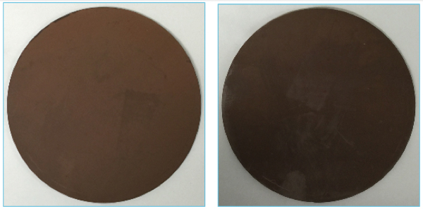
FIGURE 3 shows the copper disks coated prior to being placed in the salt fog chamber. Scuff marks were observed near the center of the Company D 7.2µm film. Birefringence patterns were observed on both of the Company C samples. Halos or rings extending from the perimeter inward were observed on the Company A samples. Honeycomb-like patterns were observed on the Company B samples, suggesting the samples were coated upside down.

Figure 3. Images of the coated copper disks prior to being placed in the salt fog chamber.
Birefringence is the double refraction of light in a transparent, molecularly ordered material, which is generated by orientation-dependent differences in refractive index.2 These differences in refractive index for Parylene C films are affected by deposition temperature and, in turn, by degree of crystallization. The degree of crystallization in polymers describes the partial alignment of the polymer’s molecular chains. Since the degree of crystallinity is affected by deposition temperature, as well as internal and external stresses, it is best to control the thermal history and stress states3 of the films in future comparisons.
FIGURE 4 shows the same copper disks after 168 hr. in the salt fog chamber. The Company D 7.2µm sample showed some signs of corrosion where the scuff marks were observed previously, proving the scuff marks were indeed damage to the film. The Company D 2.1µm sample had very minor points of corrosion. The Company C 2-3µm sample had extensive patina corrosion product over the surface of the sample. The Company C 5-6µm sample had minor points of corrosion. Both Company A samples had extensive discoloration around the perimeter, where the halos were observed, as well as darkening of most of the disk. Both Company B samples had very minor points of corrosion, but the Company B 5-6µm sample had discoloration showing the honeycomb pattern, likely due to the sample being face down during the deposition process.

Figure 4. Images of the coated copper disks after being exposed to salt fog for 168 hours.
ImageJ4 was used for image analysis on the Company C 2-3µm and the Company D 2.1µm samples for comparison and quantification of corrosion protection performance. The Analyze Particles function was used with the results summarized in TABLE 2. The Company C sample had more than 10 times the particles, and those particles occupied just over six times the amount of area when compared to the Company D sample.
Table 2. Image Analysis Data of Company C and D Coated Copper Disks for the Thinner Coating
FIGURE 5 shows another set of Company D coated copper disks that were exposed to 264 hr. (11 days) of salt fog with no evidence of corrosion. Again, the discoloration was due to oxygen penetrating the film, but moisture was blocked.

Figure 5. New samples of Parylene C coated copper disks, 7 microns thick, which were exposed to 11 days of salt fog with no evidence of corrosion.
Nitric Acid Test Results
Additional coated copper disk samples that weren’t exposed to salt fog were immersed in 10% nitric acid for 30 min. FIGURE 6 shows a Company D 2.1µm sample with no evidence of corrosion. FIGURE 7 shows a Company C 2-3µm sample that has marks resembling scratches all across the surface of the disk. Note that while the Company C sample was immersed, bubbles were observed on this sample, indicating that nitric acid was reacting with exposed copper.

Figure 6. Image of Company D coated copper disk, 2.1µm thick, after exposure to 10% nitric acid.

Figure 7. Image of Company C coated copper disk, 2 to 3µm thick, after exposure to 10% nitric acid.
Surface Roughness Test Results
Surface roughness was determined for the samples using atomic force microscopy (AFM) in the Micron Microscopy Suite at the University of Utah. Measurements were captured over 1 x 1 and 10 x 10µm areas on all of the samples, with measurements repeated for an additional two Company D coated samples over a 10 x 10µm area. Data for these measurements are shown in TABLE 3.
Table 3. Surface Roughness Determined by AFM for All Coatings

The general consensus from these data is the Company D coated samples had higher surface roughness, which is likely due to the faster deposition rate. The higher surface roughness though has not affected the performance of the Company D coating in terms of corrosion protection.
The high surface roughness may actually have other benefits in the area of LED encapsulation. In an article by Fujia Zhang et al.,5 surface roughness was affected by deposition rate with 2 µm/h resulting in 15nm valley to peak and 5.6µm/h resulting in 50nm valley to peak. The surface roughness affected LED output performance parameters. In the same article, they note that the light output from a surface with nano-rough morphology is enhanced by reducing the total reflection effect, enhanced light extraction from the silicone encapsulation of LEDs with an island-like morphology surface. In addition, by examining the radiation patterns, LEDs show stronger light extraction with a wider view[ing] angle. These results offer promising potential to enhance light output powers of commercial light-emitting devices by using parylene C layer under suitable island-like morphology nano-rough surface.
Zhang et al. also stated that higher rates of deposition lead to poorer quality films, but that hasn’t been seen by the authors. Company D’s roughest film though was 23.5nm valley to peak, which was less than half of the 50nm valley to peak observed by the investigators.
Contact Angle
Contact angles for coated samples were measured using a Ramé-Hart Instrument Company Model 190 Contact Angle Goniometer and distilled water. A contact angle is formed between the solid/liquid interface and the liquid/vapor interface produced from a drop of a liquid on a solid.
A drop with a contact angle over 90° is hydrophobic. This condition is exemplified by poor wetting and adhesiveness, and the solid surface free energy is low. A drop with a small contact angle is hydrophilic. This condition reflects better wetting, better adhesiveness, and higher surface energy.6
In general, as roughness of a surface increases, the contact angle in a Wenzel state will generally increase on hydrophobic surfaces and decrease on hydrophilic surfaces.7 In a Wenzel state, the liquid from a drop fills the voids below the liquid and thus occupies more surface area. In a Cassie (a.k.a. Cassie-Baxter) state, the drop rests upon the asperities with gas left in the voids below the drop. The surface area is less than it would be for a drop of the same volume and apparent contact angle on a flat or rough surface in a Wenzel state.8 Figure 8 shows the difference between Cassie and Wenzel states.

Figure 8. Diagram showing the difference between Cassie vs. Wenzel states.
The contact angle data for the Parylene C coated samples, as well as comparisons to alumina and native oxide on silicon, are shown in TABLE 4. All the Parylene C coated samples were hydrophobic, with the Company D samples having the lowest contact angle within the set.
Based on the information above regarding increased roughness, as well as the surface roughness data, the Company D sample would have been expected to increase contact angle. The suspected reason for the decreased contact angle was increased oxygen content at the surface of the Company D coating from process termination by venting to atmosphere, where oxygen terminates free radicals of the Parylene polymer chain and leaves an oxygenated functional group, such as hydroxyl (-OH), that decreases contact angle, increases hydrophilicity, and decreases hydrophobicity. More details on this subject will be provided in a future article.
Crystallinity by XRD
Evans Analytical Group performed x-ray diffraction (XRD) to determine the percent crystallinity of the coatings on silicon wafers. Wafers were mounted directly onto the diffractometer with clips. XRD data were acquired by grazing incidence XRD (GIXRD) on a PANalytical X’Pert Pro MRD diffractometer equipped with a copper x-ray tube and parallel-beam optics. The incidence angle was fixed at 0.3˚.
FIGURE 9 compares the data from all four samples. Superimposed on the patterns is the ICDD/ICSD (International Center for Diffraction Data/Inorganic Crystal Structure Database) diffraction reference pattern for polycrystalline silicon. There is almost no difference in these samples.

Figure 9. Comparison of GIXRD data from all four samples. Data from EAG.
TABLE 5 provides the percent crystallinity of each of the four Parylene C coating samples. D was found to be 40% crystalline, the lowest of the four, which was likely a characteristic of the deposition process. Again, since D’s rate of deposition is considerably faster than other known Parylene providers, the polymer isn’t afforded time to organize and align, becoming less amorphous and more crystalline.
Mechanical Properties
Tensile strength. The tensile strength of a material is the maximum amount of tensile stress that it can take before failure, for example, breaking. Tensile stress (or tension) is the stress state leading to expansion, and induced by pulling forces in a uniaxial manner.
Samples from Company C couldn’t be tested for tensile strength, since they were deposited either too thin or with an adhesion promoter. Therefore, the films were unable to be removed from their respective silicon wafers.
The tensile strength of the samples from Company A, B and D were determined by the University of Utah using a uniaxial tensile test at room temperature, and the data are shown in FIGURE 10. Five samples from each coating provider were tested, and both Company A and D were within the same range, while the samples from Company B were about 20% lower.

Figure 10. Maximum tensile strength of films from Company A, B and D. Data from University of Utah.
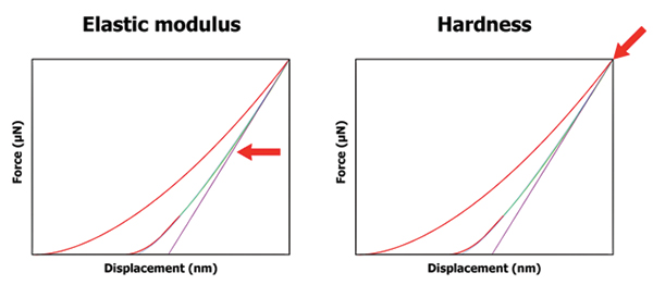
Hardness and reduced modulus. During a nanoindentation test, the nanoindentation probe is driven into a sample and then withdrawn by decreasing the applied force. The applied load and depth of penetration into the sample are continuously monitored. A load vs. displacement curve can be generated from the data, and from that data sample hardness [H] and reduced modulus [Er] can then be calculated.10 FIGURE 11 shows graphical examples of force-displacement curves generated with nanoindentation with the types of parameters that can be obtained with the data.

Figure 11. Examples of force-displacement curves generated with nanoindentation with the types of parameters that can be obtained with the data.12
Hardness is a measure of how resistant solid matter is to various kinds of permanent shape change when a compressive force is applied. The reduced modulus accounts for the elastic displacement in both the specimen and indenter.11
Hysitron provided hardness and reduced modulus data for the films using a TI 950 TriboIndenter with Diamond Berkovich and 5µm Conical Probe with two main test methods: quasi-static nanoindentation and frequency sweep test.
The quasi-static nanoindentation testing procedure consisted of:
- A partial-unloading load test with a peak force of 1000µN and a single test consisting of 20 cycles of loading, holding, and unloading segments.
- A quasi-static test with a peak force of 150µN for Samples 2, 3, and 4 and 25µN for Sample 1 and a single test consisting of 5 sec. loading, 2 sec. holding, and 5 sec. unloading segments.
FIGURE 12 shows the reduced modulus and hardness of the samples at different contact depths. The Company C sample didn’t correspond with the other samples because of substrate effects, since the coating was thin, due to the sample being coated on the opposite side than intended. The other three samples:
Company A, B and D had similar results, indicating the mechanical properties were due more to the type of material than the coating provider.

Figure 12. Reduced modulus (top) and hardness (bottom) of the samples at different contact depths. Data from Hysitron.
FIGURE 13 shows the average hardness, reduced modulus, and the contact depth of the samples obtained from the quasi-static indentation tests. Again, the Company C sample deviates from the rest due to substrate effects from the sample being too thin. The error bars represent one standard deviation. Sample 1 appears to have higher reduced modulus and hardness, which is likely a result of the substrate effect. The samples are the same as in Figure 12.

Figure 13. Average hardness, reduced modulus and the contact depth of the samples obtained from the quasi-static indentation tests. Data from Hysitron.
Process control. Some of the providers didn’t follow the proper instructions when depositing the coatings on the samples, which made comparisons difficult. The issues encountered included coating the wrong side of samples, coating at the wrong thickness, the use of adhesion promoters, and even when sample runs had to be repeated, a few of the issues still occurred.
Conclusions
In the salt fog test, the coatings performed well when deposited as requested and without physical damage. In the nitric acid test, the coatings performed well when deposited well. Surface roughness, contact angle, and crystallinity values for Company D’s coating were different from the others, but didn’t affect environmental protection performance. In mechanical testing, tensile strength, hardness, and reduced modulus, all the coatings, when deposited to an appropriate thickness, had similar results.
Ed.: Company D sample was developed by HZO.
Acknowledgments
Raleigh Cao was very helpful with testing, as well as interacting with the University of Utah and Hysitron. Becky Alseth was very helpful in researching competitors and business analysis. David Voyen was very helpful in interacting with the coating competitors. Yang Yun was very helpful in managing the project.
References
1. Altana, “Introduction in Adhesion Measurement,” Theoretical Information on Appearance, Color and Physical Property Testing, June 18, 2015.
2. Nikon, “Introduction to Optical Birefringence,” Microscopy U - The Source for Microscopy Education, Aug. 27, 2015.
3. Jay J. Senkevich and Seshu B. Desu, “Morphology of Poly(chloro-p-xylylene) CVD Thin Films,” Polymer, 1999.
4. Wayne Rasband, ImageJ. U. S. National Institutes of Health, Bethesda, MD, US, 1997-2014.
5. Xiyuan He, Zhang Fujia and Zhang Xu, “Effects of Parylene C Layer on High Power Light Emitting Diodes,” Applied Surface Science, June 29, 2015.
6. Hysitron, “Probe Calibration Service Document,” June 26, 2015.
7. Ramé-Hart Instrument, “Roughness and Contact Angle,” September 2010.
8. Ramé-Hart Instrument, “Wenzel and Cassie,” September 2008.
9. Ibid.
10. Hysitron, “Probe Calibration Service Document,” retrieved June 26, 2015.
11.Wang, W., and K. Lu, “Nanoindentation Measurement of Hardness and Modulus Anisotropy in Ni3Al Single Crystals,” Journal of Materials Research J. Mater. Res. 17.09, 2002.
12. Kathy Walsh, Ph.D., “Nano- and Micromechanics,” Advanced Materials Characterization Workshop, 2014.
Sean Clancy, Ph.D., is chemist and project manager, HZO (hzo.com); This email address is being protected from spambots. You need JavaScript enabled to view it..


