A guide to understanding the base material and copper options.
Developing a rigid-flex printed circuit board is difficult enough, but when that PCB has high-speed signals as well the design can get complicated. For example, how do you determine what’s more important: high-speed signal integrity or the flexibility of the circuits?
PCB design is all about managing tradeoffs in the planning and layout stages, and a hybrid high-speed and rigid-flex design requires care when making these tradeoffs. To be successful when designing a complicated rigid-flex PCB with high-speed signals, follow a specific set of best practices.
Before beginning the design process understand the intended application of the board and how the rigid and flexible sections will be used. This will largely determine whether the emphasis will be on signal integrity or the long-lasting flexibility of the circuitry.
The first question to ask is whether the rigid-flex board must bend and fold in daily use. If the answer is “yes,” select materials that provide the best product reliability and longevity. This type of board is called a “dynamic flex.” Of course, high-speed signal integrity cannot be ignored when designing a dynamic flex board, but PCB reliability should come first in this type of application.
The tradeoff here is that to control the impedance of a signal path and maintain good signal integrity, most designers route high-speed signals over solid copper ground planes. Solid, unbroken copper ground planes are not very flexible, however, and can impact the reliability of the PCB.
On the other hand, if the flexible circuitry will only be bent or folded occasionally – perhaps during manufacturing or service – the design effort can focus on ensuring the signal integrity of the high-speed signals. This type of PCB is called a “flex-to-install” board.
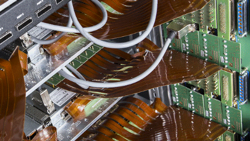
Figure 1. Rigid-flex circuit anchored during installation.
A flex-to-install PCB design can incorporate beefier ground planes than if the design were for a dynamic flex board. Thus, the emphasis will not be on the reliability of the flexible board materials but on providing solid signal return paths that preserve signal integrity.
In either case the cost to manufacture the PCB must be considered. Having a limitless budget makes many things possible, but that luxury does not exist today. The final PCB design will not only have to meet performance goals but also be cost-effective.
Once this analysis is complete, define the specific design rules and layer stackup requirements that will be used to design the board. Below, we’ll analyze some of the best design rules to use when designing dynamic flex and flex-to-install PCBs and show how to set up a proper layer stackup for impedance control and signal integrity.
Designing a dynamic flex PCB. As noted, a dynamic flex PCB is one that will bend constantly during use. The challenge is copper naturally fatigues and will eventually harden and crack. To accommodate high-speed signals, generally the board should have an unbroken copper ground plane, but unbroken copper layers are not as flexible as hatched layers. As a result, the ground plane on the flexible portion of a dynamic flex board is more likely to crack and fail.
Copper thickness and foil production methods also play a role. The typical electrodeposited copper foils are thicker and more prone to fatigue failures in flexible circuits. While providing a nice ground plane, they inevitably reduce longevity. Annealed copper is thinner but is more flexible and enduring, and can still provide for good signal integrity.
Annealed copper is more durable than standard copper but costs more. This option might be selected for applications where signal integrity is the highest priority.
To reduce copper costs and preserve flexibility, use cross-hatched polygon ground planes (FIGURE 2). The drawback to hatched polygons is reduced signal integrity. Compared to PCBs that have solid ground planes, PCBs with hatched polygon ground planes increase the rise and fall times of high-speed signals, as return currents are forced to meander around the hatch.

Figure 2. Process of annealing copper.
Several measures can improve signal integrity. For example, the effect a hatched polygon ground plane has on rise and fall times varies based on the position of high-speed signal traces with regard to the ground plane. That being the case, providing localized solid return paths directly under high-speed traces can be a good compromise. If this option is chosen, the return path should be five to 10 times the width of the signal trace.
Once the board materials have been chosen, the layout stage may proceed. At this stage, the number of layers the PCB will have and how they will stack up is determined.
Using the ECAD tool, specify the layer type, the material type, the material thickness, and where appropriate, the dielectric constant of the material. With this information, the ECAD tools can make impedance calculations that will help ensure the integrity of high-speed signals.
Design rules are also specified at this stage. For example, specify the impedance of a high-speed signal path remains constant over the length of that path. This will tell the ECAD tool to automatically change trace widths in order to match the signal line impedance between rigid and flexible sections.
Be careful, however, not to go overboard with design rules. Many engineers use overly stringent design rules when designing high-speed PCBs. For example, there often is more space to: “length tune” than is first thought. Using overly stringent design rules can make boards more complex, and therefore more expensive to manufacture.
Designing a flex-to-install PCB. Compared to designing a high-speed dynamic flex PCB, designing a flex-to-install board is a walk in the park. Flex-to-install PCBs are bent only during the initial installation or during servicing, so the focus can be on providing high-speed signal integrity and not so much on PCB reliability.
Solid copper plane layers and a very thin polyimide film can be used in flex-to-install boards because these boards need not flex as many times as a dynamic flex PCB. This combination provides good signal integrity through the flexible portion of the PCB.
How the PCB will be installed is important. Most flex-to-install designs tend to be for high-volume applications, and this often means automated assembly. The designer must make sure there are no PCB assembly issues or system assembly issues. High-volume products are often machine-assembled, so it’s critical the PCB be designed for automated assembly.
It’s also imperative to control the impedance of signal lines by choosing the right materials. Often, the rigid portion of a high-speed PCB will use an expensive dielectric material. The flexible portion, on the other hand, will use a polyimide film that has a different dielectric constant. In this situation, expect the trace widths on the rigid portion of the PCB to be different from the trace widths on the flex portion of the PCB.
Material thickness also has an effect on impedance. The thinner the dielectric the more capacitance a signal line will have. This capacitance will affect the high-speed performance of the board.
Another issue is the flexible substrate forms a part of the rigid board. While polyimide film and rolled annealed copper provide high signal integrity in the flexible portion of the PCB, there may be a mismatch with the dielectrics in the rigid portion of the PCB. It may also be difficult to place and solder components to this film.
The layout of a flex-to-install PCB is similar to the layout of a dynamic flex PCB. Set up the layer stacks in much the same way and apply similar design rules.
Different materials and different thicknesses will be used, but the ECAD tool should automatically control signal line impedances by varying the trace widths between rigid and flexible sections of the PCB. And, similarly, be careful about applying overly stringent design constraints that can surreptitiously drive up PCB costs.
Designing high-speed PCBs is hard enough. When those boards need to flex as well, it only gets tougher. Take care to analyze the requirements upfront. This will help guide the appropriate tradeoffs. Choosing the right tradeoffs and using good ECAD tools will enable successful designs of high-speed, rigid-flex printed circuit boards.

Figure 3. Cross-hatching can help reduce copper costs and improve flexibility while at the same time preserve signal integrity.
Ben Jordan is senior product manager for PCB design and 3D modeling products at Altium (altium.com); This email address is being protected from spambots. You need JavaScript enabled to view it..
Ed.: The original article contained a different Figure 1. This version has the correct figure.


