When prepping files for manufacturing, the more detail the better.
CAD/CAM data have taken over the world of electronics. Since design and manufacturing are driven by data, much of what is accomplished on manufacturing floors has been standardized. However, the assembler’s challenge has not only been to create the machinery and processing, but also to keep up with new-generation processors running at incredible speeds, which require special considerations. Along with “traditional” CAD/CAM data, there is still a need for textual information in the form of notes and special detailing to provide a complete engineering design package and ensure a smooth manufacturing process.
Much time has been spent designing the board and getting it “just right.” It is critical to provide the manufacturing partner the information needed to meet the design intent. Without guidance from the designer, the fabricator will either make assumptions or delay manufacture.
Let’s look at what composes a complete PCB data package and examine the notation and graphic documentation that must accompany it.
File naming convention. Avoid nondescript or vague names like “TOP.GBR” for files. Without specificity, the purpose of a data file name will surely be confused. As shown in the following examples, incorporating a part number and revision into the file name links the file to a document control system. Adding a clear functional description to the file name will surely help anyone using the data realize its purpose without having to view it:
- 424242_B_LAYER_1.PHO
- 424242_B_DRILL.DRL
- 424242_B_FABDWG.DXF
Gerber data files for all required PCB artwork layers. This is the starting point for graphic CAM tooling. Referred to as “artwork,” the supplier modifies these data to conform to its manufacturing capabilities to meet finished feature requirements specified in the fabrication drawing (FIGURE 1). After layout is complete, the software can output these files, each of which will become the basis for the etched copper pattern for each PCB layer. When outputting Gerber file data, use the very common RS-274X output. This selection utilizes special technology referred to as “embedded apertures” to create artwork shapes.
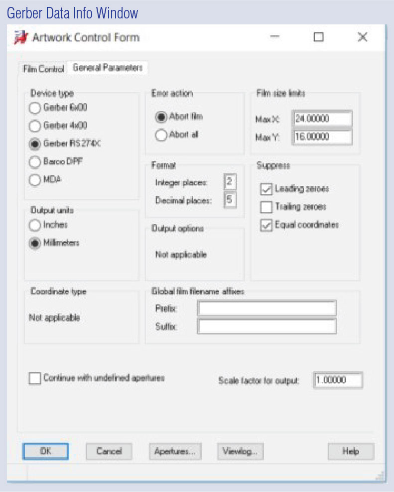
Figure 1. When outputting Gerber data, RS-274X is recommended.
Industry standard design continuity verification output. IPC-2581 or ODB++ design output and an IPC-D-356 format netlist will help the fabricator verify the artwork matches the design intent electrically before and after fabrication. The more intelligent and comprehensive the data, the better.
Industry standard drill file. Drill files define the nominal x,y position of the holes, but the numeric values output from CAD software define the finished hole size, not the drill size. Drills must be larger than plated holes specified to compensate for plating thickness; the fabricator will select the appropriate drill size. A common output format is Excellon.
Neutral database file. Providing the source file for the complete design database allows a fabricator to access the source data needed to determine design intent. Unlike “dumb” graphic Gerber data, source data provide intelligent data, net names, and connectivity information, which can be helpful in determining artwork anomalies and moving the design through the CAM process quickly. Intelligent source database formats are best output in IPC-2581 or ODB++, but some systems accept ASCII output of the original layout database.
PCB Documentation
There are other aspects of the design the CAD data cannot address alone. For instance, CAD data define the shape of an exposed component land, but not the metalized finish. It is critical to understand graphic CAD data define mostly geometric, nominal values for the features shown. There are no perfect manufacturing operations; every bit of CAD data will be subject to manufacturing tolerances.
How will the effect of manufacturing variance and so many other aspects of the design be addressed? Data and machinery run the PCB process, while graphic PCBA documentation is required to start the process. Graphic PCB documentation also helps to close out and finalize the PCB process by giving the inspection stakeholders a graphic example of what the finished PCB will look like and provides notes and specification for its final electro-mechanical configuration.
Several basic documentation elements need to be included in the fabrication drawing. They are listed below.
Pictorial. CAD data must be accompanied by textual fabrication specifications, which are best documented in an engineering drawing. The fabrication drawing serves less to indicate how a PCB is to be manufactured and more to specify how the PCB shall be laid up. CAD data can define nominal values for features such as drill geometry and the PCB outline.
Drill symbols. Drill symbols are shapes or textual characters generated by the PCB layout software to graphically show a hole’s position on the PCB. When selecting symbols for drill sizing, always use a unique symbol for each type of hole containing the same attributes. For instance, several 0.023" (0.58mm) diameter holes may be required on a PCB. If the holes are alike with regard to plating requirements and hole diameter tolerance, they may be assigned the same symbol. However, if there is a different attribute, such as a non-plated condition or a different tolerance requirement, the hole of the same size will require a different symbol, which will need to be reflected on the drawing accordingly.
X0Y0 datum feature. The X0Y0 datum is a hole on a PCB that is preferably located in the lower-left corner of the design.
Dimensions and tolerances. Designation of the origin point (X0Y0) for the design database is relative to practical interface points on the PCB. Dimensions and tolerances shall originate from X0Y0 on the PCB.
Fabrication drawing dimensions do little to communicate to the supplier how to fabricate the PCB. The PCB design tool output (CAM) data do this. Fabrication drawing dimensions are used by manufacturing and inspection personnel to gauge the accuracy of the process and machinery. Accuracy, expressed by the definition of tolerance values, must be documented on the fabrication drawing for the supplier to measure their success and adjust the process as required. CAM data do not include the establishment of tolerance zones and, therefore, have no bearing on whether a snap-fit feature will work at next assembly.
PCB stack-up detail. A stack-up detail provides imperative, upfront, cost-related information to your purchasing department and the supplier’s quoting department before the fabrication process ever begins. This detail documents a generic view of the vertical design intent: the layer count, the thickness of the copper layers, the dielectric materials in between, and the presumed thickness and dielectric properties of the solder mask material covering the outer-layer surface copper (FIGURE 2). For controlled impedance, a stack-up philosophy is recommended that permits the fabricator to vary the dielectric constant of materials, trace widths and spacing to achieve the specified impedance. This will permit use of materials of wider availability and is critical to improving the supplier’s ability to deliver the highest performance at the best cost.
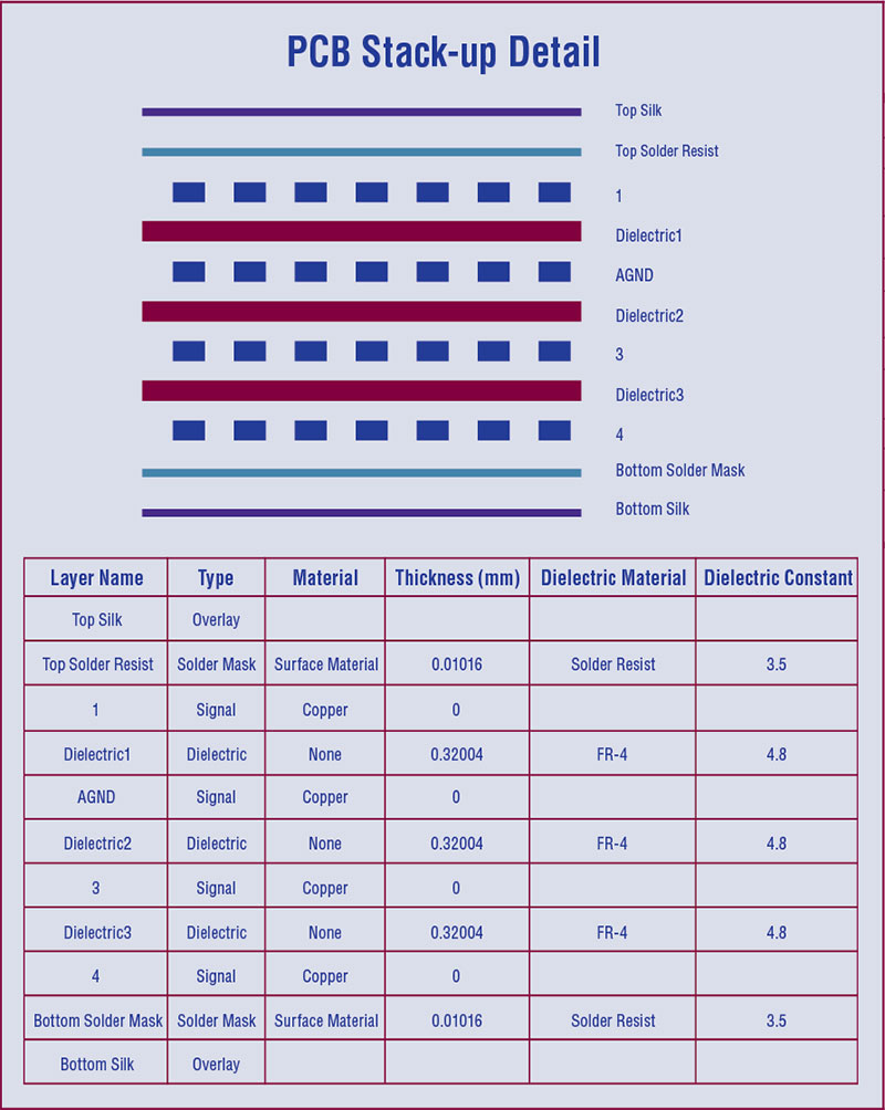
Figure 2. The stack-up documents the layer count, copper thickness and materials.
Panel processing. When the PCB design is set up for panel processing, the PCB image is multiplied several times in order to process many PCBs on the same manufacturing panel to maximize panel yield. If the design will be fabricated and assembled at external facilities, no v-score or tab-route detail is needed. Manufacturers will add these.
V-score detail. Typically, it is uncommon to provide a v-score detail on a fabrication drawing. A fabrication drawing should describe the finished part and, therefore, should not show extra processing material, unless required. If required, it is because the project stakeholders are intending to process the PCB in-house. The in-house assemblers will need manufacturing assembly arrays with v-score cuts between the straight edges of the PCB to provide rigidity during assembly operations (FIGURE 3). It’s best to always check with both the fabricator and assembler for optimal v-score parameters.
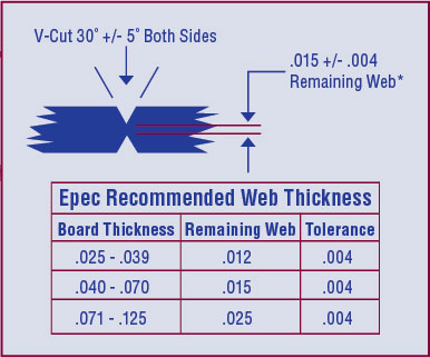
Figure 3. V-groove detail shows the scoring location and depth.
Tab-route detail. As with v-score detail, the tab-route detail is provided only if there is in-house assembly processing. Tab-routing is used to support the PCB in the assembly array with short breakaway tabs when straight edges are not available on the PCB, or a smooth (routed) machine finish is required (FIGURE 4). The best source for tab-route detail information is the assembler, because it controls the process of excising (depaneling) the finished boards.
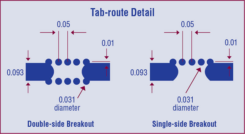
Figure 4. Tab-route details display where breakaway tabs are used.
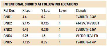
Intentional shorts table. Sometimes it is necessary to connect multiple signals at a specific point. When a net with a significant name needs to connect with another net of a different name, a designer will often use a “bond” part to connect the nets. This bond is a copper shape that makes the connection and can trick the design rules checker. However, when the connected copper shapes are compared with the IPC-D-356 netlist, a red flag is raised at the fabricator’s CAM department. The common practice of net joining will almost always cause a stop order, unless it is described on the drawing in detail. The manufacturer does not know if the “short” between multiple nets is intentional or not. An Intentional Shorts Table (TABLE 1) can be used to effectively communicate important information of bond reference designator, net-names, x-y location, and layers to the supplier’s CAM department upfront, reducing the need for stop orders.
Table 1. Intentional Shorts Table
Outline and thickness. Overall PCB length and width may be shown as a reference on the fabrication drawing if the features need not be inspected. A note pertaining to the minimum radius for internal corners and overall profile tolerance may be specified in the fabrication notes.
Impedance specification. Impedance-controlled designs require control of four physical variables in the stack-up:
- Trace thickness
- Trace width
- Trace distance from reference plane(s)
- Dielectric value of the material.
A designer may use a basic field solver or impedance calculator to determine trace widths and spacing to be used for impedance requirements (FIGURE 5). At the start of the layout, the designer should do a feasibility check to select the optimal trace widths for impedance-controlled lines. Be sure to validate the values in the stack-up with the fabricator. Use care when adding information to the stack-up detail regarding three of the four variables mentioned above. Finished copper thickness is an important consideration regarding the various conductors’ current-carrying capacity. However, to optimize DfM, allow the fabricator to adjust the values of trace width, distance from reference plane, dielectric constant of the material (Εr), and material sources.
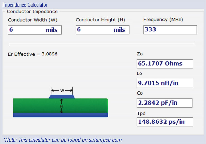
Figure 5. Impedance calculators take into account trace widths and spacing.
Conclusion
CAD/CAM data have replaced the need for human contact with the features comprising the finished PCB during manufacturing cycles. Manufacturing stakeholders rely on data automation and machinery to create fine lines and complicated mechanical PCB features. A common assumption is the manufacturing processes and machinery of today create hardware that perfectly matches the nominal layout. However, it is a sad fact that PCB designs continue to be revised due to lack of understanding in design specification, namely textual and graphic documentation.
Data that drive high-tech machines are strictly nominal. Machines and processes have a tolerance that will yield parts that will rarely, if ever, be exact. In design, adding a variance factor to the layout can prevent assembly conditions that are too tight or loose.
Data have other shortcomings. CAD data will not automatically color solder mask to be blue or legend ink to be yellow. Embedded CAD data will not automatically select RoHS materials or automatically pull high temperature grade material into a stack-up during lamination. Completing fabrication still relies heavily on textual and graphically detailed information provided on a comprehensive fabrication drawing.
A sufficiently embellished fab drawing will fill in the blanks embedded data leave out. And while CAD/CAM data tell the manufacturer’s machines what to do, graphic and textual information provided on the fab drawing guide the inspection department in checking how well it did.
This excerpt of The Hitchhiker's Guide to PCB Design was written by EMA Design Automation. Download to learn more about PCB design stakeholders and real-world, actionable PCB design tips from industry experts (go.ema-eda.com/pcbguide).


