DfM considerations for ensuring a balanced board.
Due to its effect on both a PCB’s electrical and mechanical performance, a sound PCB stackup strategy is vital to creating a reliable PCB. Part one of this two-part series discussed cost-adders. Here, we discuss some added DfM considerations to ensure a manufacturable, flat PCB.
Balancing the stackup. PCB warping can occur in a board when a designer is unaware of or does nothing to mitigate mechanical stresses. These can build up when laminating dissimilar layers of copper with various thickness combinations of epoxy-glass laminates.
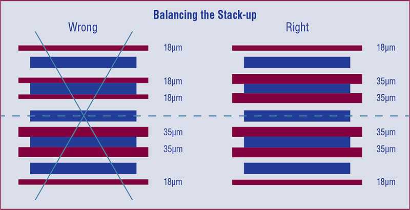
Figure 1. Stackup balancing.
Ensure materials on each side of the PCB stackup centerline are matched. If the stackup is laminated with disproportionate materials and material thicknesses, the unbalanced stackup will experience warping due to built-in stresses incurred after heated lamination and cooling.
Core construction. Core construction builds up a multilayer PCB. Double-sided cores are printed and etched, then bonded together with a material called prepreg or “B-stage” material. It remains tacky as board layers are stacked up in a press and cures when heat and pressure are applied. The process is mostly utilized on microwave PCBs, where very expensive, high-tech microwave laminates are combined with low-cost laminates to achieve a compromise solution for performance and price. Made up of core materials on the outer-layers, this type of stackup is called a “core build.”
Foil construction. The most common method for laminating multilayer designs is the foil construction method combined with a sequential lamination process. In sequential lamination, cores may be individually printed, etched, and even drilled and plated prior to being laminated together with other cores. Individually selected sheets of copper and prepreg laminate materials create a diverse combination of layer interconnects. The foil construction methodology also has the advantage of “dialing in” distinctive combinations of epoxy-glass weaves that use unique resin-to-glass ratios, yielding exceptional dielectric properties to help control trace impedance as required.
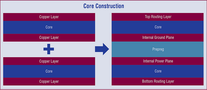
Figure 2. Core construction stackup.
Specifying impedance. It is not enough to simply specify an impedance on PCB traces. The impedance must be achievable in manufacturing, based on good stackup design. The PCB fabricator is allowed three ways to adjust trace impedance accurately on a PCB: dielectric and value of the material, trace distance from reference plane(s), and trace width and spacing. When designers select trace widths based on values determined by an impedance calculator, the manufacturing team can easily adjust the dielectric strength and thickness of the prepreg materials in stock. Different prepreg materials can be used to adjust the trace distance from the reference plane to achieve the specified impedance value, and trace width and spacing may be dialed in through the CAM department. However, the PCB fabricator can only achieve impedance this way if it is noted on the fabrication drawing. The note must state the three specific characteristics may be varied.
Sometimes specialized customer engineering requirements will not tolerate variations in physical composition or structure. Hybrid material-controlled stackup specification is less common and usually done when PCBs will be used in space or other specialized circumstances. This methodology is very expensive and results in long lead-times due to the need for specialized materials and processes. If material-controlled stackup methodology is not required for performance, it must be eliminated from the design process, as it will mostly yield higher-cost parts or a no-bid on a request for quote.
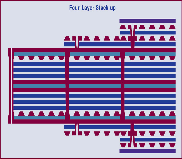
Figure 3. Four-layer board stackup.
Trace width vs. copper thickness. Sometimes the decision to add layer pairs to a PCB stackup is based on the amount of available routing space. One way to handle this is to examine whether shrinking the trace widths and spacing would permit all the routing to fit. However, this option must be cross-checked with the PCB fabricator. The print-and-etch factors for trace widths must stay proportionate to each other to some extent, meaning as the trace-width is reduced, the height (or thickness) of the trace must shrink proportionally along with it, and must be reflected in the PCB stackup detail. Due to the nature of the PCB print-and-etch processes, the acids attack the sides of the traces in contact with the substrate material more aggressively, causing a trapezoidal effect. If the copper thickness is not reduced, the width of the copper at the base may become too narrow and fail.
Balanced etching between layers. Besides etching considerations for trace routing, imbalanced etching of larger copper areas of the PCB can contribute to layer stress and warpage and will cause an inherent balancing challenge for the fabricator. Commonly, core laminates are supplied with copper foil laminated evenly to both sides. The laminated copper expands and contracts at a much different rate than the epoxy-glass laminate, but when the copper exists on both sides of the epoxy-glass equally, the stresses are evened out, permitting the core to remain flat.
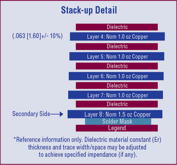
Figure 4. Stackup detail.
Challenges are introduced when a large percentage of the copper is only etched off one side of the core. If there are dense copper patterns on one side, try including copper “fill flooding” by using ground fills on the opposite side to balance out the copper on each side. In the case of multilayer stackups, do not randomly flood every layer with copper flooding for the cause of balancing the stack. In general, every signal layer deserves a solid return path laminated adjacently to it in the stackup for signal integrity purposes.
PCB flatness is achieved by sound design, not brute force. While it would be easy for the PCB fabrication engineers to mechanically warp boards in the opposite direction to meet any flatness specifications for problem designs, it would also be unethical. Upon experiencing heat in the wave solder or reflow oven, an unbalanced PCB will again warp to its unconstrained equilibrium, and the problem will be once more exposed.
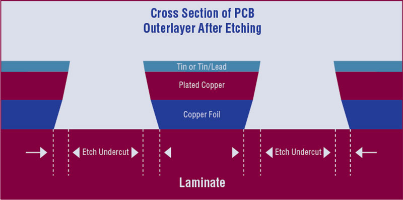
Figure 5. Cross-section of PCB outlayer after etching.
Keeping DfM considerations in mind when creating a PCB stackup will help decide critical issues in a project. Properly balancing the copper in the design stackup during layout is the best preventative method to achieve PCB flatness and a manufacturable board.
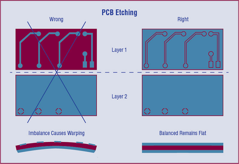
Figure 6. Effect of balanced construction on board flatness after etching.
This excerpt of The Hitchhiker's Guide to PCB Design was written by EMA Design Automation. Download to learn more about PCB design stakeholders and real-world, actionable PCB design tips from industry experts (go.ema-eda.com/pcbguide).


