
Using buildup layers and premium FPGAs to deal with SI challenges.
Where signals need return vias, component vendors often do most of the work. Let’s look at a PCI Express differential pair, starting with a standard connector, showing its pinout but not its body. (I’ll cover the connector body in a moment.) The signal pin assignments are also standardized.
FIGURE 1 shows a through-pin component. The two sides of the differential pair (marked P and N) are close to ground pins. There’s some differential coupling between the P and N pins, and the ground pins create returns in the Z dimension, just like ground planes do for traces.
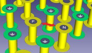
Figure 1. Differential pairs (marked P and N) on a connector.
The connector body works in a similar way. FIGURE 2 shows a small area of the connector, mounted on its footprint. Inside the body, the differential pair has ground metal on each side.
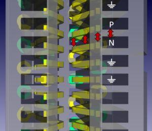
FIGURE 2. An inset of the connector, mounted on its footprint.
This pair could already be routed from BGA to connector on, say, the top and bottom layers, without adding any other vias. If another layer change is needed for a signal like this, the designer must decide on signal via-to-via and return via spacing.
Or do they?
Let’s look at the BGA itself. In this case (FIGURE 3), its balls are on a 1mm grid, fanned out to vias at even spacing. Markers on the vias show the differential pair (N and P) and surrounding ground vias. These signals are on a special high-speed transceiver bank on the FPGA. If another layer change is needed, one way to decide on spacing is just to copy this pattern.
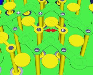
Figure 3. A BGA with markers on vias to show the differential pair and surrounding ground vias.
Alternatives to return vias. You can’t backdrill vias inside the area of a BGA like this, so the alternatives are blind vias or buildup layers. In any case, you often need buildup layers to achieve the high route density that BGAs like this demand. All that’s required then is to restrict routing layers.
• Buildup vias are also much smaller than conventionally drilled vias, and their correspondingly smaller parasitic resistance, capacitance and inductance yield better performance, even on slower signals.
• Blind and buried vias add process steps and expense.
• Backdrilling is mainly suited to larger via geometries, so its use is limited, but it’s effective for signals that are a little less critical than PCI Express, such as some SDRAM buses.
Premium components like the FPGA mentioned here include features to help signals fly true. Some of the latest BGA footprints are so fine-pitched that many signals connect only through via-in-pad to innerlayers, with no room for traces between pads.
Now that EDA environments work in three dimensions and with high levels of detail, it’s much easier to visualize where signals are going and what will help or hinder them.
John Berrie is PCB design specialist at Zuken (zuken.com); This email address is being protected from spambots. You need JavaScript enabled to view it..


