Existing advanced methodologies for cross-discipline co-design, and new methodologies for resolving their gaps.
As products deliver more functionality, requiring greater electronic and mechanical design complexity, while also shrinking in size, packaging and electronics assemblies are becoming more tightly integrated than ever. Increasingly, packaging must take into account the physical properties of the electronics, while the electronics design is subject to even tighter mechanical constraints. Teams working on the electronic and mechanical aspects of the design need to continuously exchange design information to avoid wasting time on a direction incompatible with another discipline. Exchange of design information is currently limited, however, because the mechanical design is nearly always done in 3D, while the electronic design is done one board at a time in 2D or 2.5D. Neutral file formats such as Intermediate Data Format (IDF) pass printed circuit board data, yet the need to flatten the mechanical design before it can be used in an electrical computer-aided design (ECAD) system means that much of the design information is lost in translation.
New generation ECAD systems address this challenge by providing multi-board and native 3D design capabilities, along with direct translation to leading mechanical computer-aided design (MCAD) systems, enabling complete packaging and electronics assembly information to be transmitted between different disciplines in a fraction of the time required in the past. New methodologies for electromechanical collaboration remove barriers between mechanical and electronic design. This approach enables design teams to accurately exchange data and design to the necessary design specifications and constraints, reducing design iterations and error-prone steps in the design process to help reduce product development cost and time-to-market.
Increasing need for electrical/mechanical design collaboration. Electronics are increasingly being embedded into a range of products that were traditionally purely mechanical, ranging from wristwatches to eyeglasses. Meanwhile, traditional electronic products such as cellphones and PCs are gaining many new electronic and mechanical capabilities at the same time they are being reduced in size and taking on more stylish aerodynamic shapes. This new era of aerodynamic packaging is not only shrinking mechanical and electrical tolerances but also introducing complex 3D contours. The electrical and mechanical aspects of products such as these are designed by electrical engineers focusing on voltage, current and connectivity, while mechanical engineers and industrial designers focus on style, fit and weight. The combination of increasing capabilities, shrinking size and more complex external shapes means that electronics must increasingly take into account the shape of the package, while the mechanical design is more dependent than ever on the physical aspects of the internal electronics. As an example, board assemblies now often hold external electronic components such as displays, keypads and connectors that are exposed to the user, eliminating the traditional boundary between the package and the internal electronics.
Traditionally, mechanical and electrical design processes have been separate with design data being exchanged between the different disciplines at critical stages. The trend toward increasing design complexity and closer integration of electrical and mechanical design increase both the amount of data and the frequency with which data needs to be exchanged. Often as many as a dozen design iterations are produced per day, each of which needs to be translated from the mechanical to electrical environment and vice versa. The challenge is particularly great when flexible PCB designs are used in order to fit inside a geometrically complex housing. Flex lines and bend lines often change on a regular basis and need to be frequently exchanged between ECAD and MCAD.
Data exchange challenges. IDF and DXF are the most common methods of moving geometrical information between ECAD and MCAD systems. IDF is limited to sharing the board shape, basic component shapes and locations, hole definitions and locations and keep-in/keep-out areas. IDF does not track much of the information critical in leading-edge design such as flex lines and bend lines. IDF represents the board shape at a given point in time and does not keep track of changes. The new IDX neutral file format goes one step further by tracking incremental changes to the baseline and giving designers the ability to evaluate the effect of changes before accepting them.
The greatest obstacle to effective communication of design data is that nearly all MCAD systems today are 3D, while most ECAD systems are 2D with some type of 3D viewing capability. The need to convert from 2D to 3D and back with each design iteration, along with the inability of electrical designers to define 3D geometry, impedes the design flow. Enclosures are increasingly migrating from orthogonal to more complex curved shapes that cannot be accurately depicted in a 2D system. So electrical engineers often either need to manually track the shape of the enclosure, which is only practical for simple shapes, or write complicated scripts to provide an accurate representation of a 3D shape.
ECAD systems typically operate on one PCB at a time, but most products contain multiple PCBs. Multi-board designs greatly increase the challenge of the translation process because of the need on the electrical side to track connectors and other common points between boards and the need to manually communicate this information to the mechanical team. Inaccurate or incomplete information in many cases means batteries don’t fit; mounting screws create shorts against PCBs, and connectors don’t mate with packaging openings.
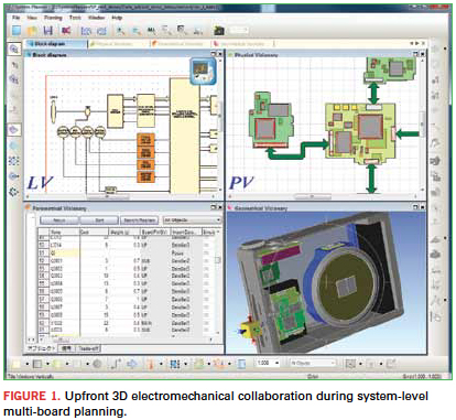
Multi-board 3D design environment. The new generation of ECAD systems offers a full multi-board 3D design environment. The mechanical enclosure can be imported directly into the layout, improving the chances for correct single or multi-board design. During layout, a wizard imports the 3D enclosure model and specifies all associated PCBs. Then, the PCBs are laid out with the enclosure in real-time, optimizing placement capacity and capturing interference violations earlier in the design process.
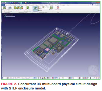
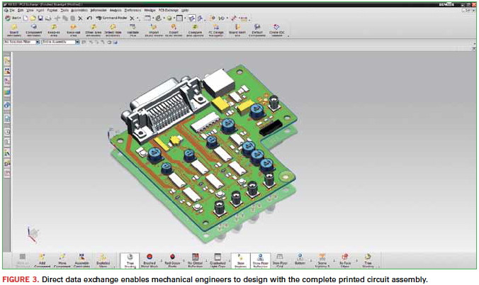
Interfaces with the leading MCAD systems make it possible to perform concurrent mechanical and electrical design. 3D parametric libraries are shared between the ECAD and MCAD systems. Electrical engineers can design to the true native 3D constraints as defined by mechanical engineers, while mechanical engineers in turn have access to the true 3D board design so they can accurately place and conduct interference checks during board layout. The STEP and SAT (ACIS) file formats are used to communicate 3D mechanical constraints and also to share real 3D electrical and mechanical components/assembly between ECAD and MCAD (Figure 3). Additionally, by importing accurate 3D enclosure and component models, engineers can create board outlines, design to the actual 3D enclosure as a constraint, and conduct interference checks to reduce data exchange and optimize multi-board floor planning and design. The new environment allows design teams to lay out complete system designs – from prototypes to complex, multi-board systems – using a single tool. Engineers and designers can flow through the design process optimizing form, fit and function of single and multi-board systems, maximizing design reuse, without reentering upfront planning data into the design tools during detailed design. Regular exchanges on board profiles for flex boards, bend lines and bend areas expand the level of detail and constraints that can be considered on the design.
Working with the exact product shape makes it possible to, for example, fit more functionality into the domed-shaped package of a pacemaker than could be accomplished with an orthogonal approximation. 3D ECAD design enables more accurate alignment of connectors so that they precisely fit openings on the enclosures. Electrical engineers can design multiple boards within a single model to ensure precise positioning of angles, shapes and cuts needed to avoid interference and to mate connectors. Rule checks support multi-board design for physical connector mismatches, I/O checks to ensure continuity between boards, and checks for duplicate references throughout the system.
Domain-level management. Finally, the latest ECAD systems provide domain-level management with metadata-based data handling at the file level, including explicit definition and tracking of object versions together with the controlled progression of changes through the development lifecycle. For development departments, this ensures that relevant changes are consistently highlighted and then distributed to all consuming models that require the change, even if the consuming models are located across many locations and sites. Change management support across the engineering process enables users to communicate individually with related teams, projects, designs, components or even across disciplines. It closes the loop on workflows by automatically notifying the relevant users or change groups and then provides them with acknowledgment and confirmation of the receipt of changes. History management capabilities perform concurrent changes to components throughout the product lifecycle, with full tracking and transparency.
Traditionally, mechanical and electrical/electronic design processes were separate, with design data being exchanged between MCAD and ECAD systems at critical stages. Limitations in the data exchange and lack of codesign functionality resulted in extra design iterations, driving up development time and cost. A native 3D ECAD environment opens the doors to breakthrough ECAD/MCAD collaboration. Electrical engineers can import a mechanical housing to a single or multi-board design and accurately place and conduct interference checks during board layout. The result is a reduction in design time, fewer errors and the ability to fit more functionality into a smaller package size.
Humair Mandavia is executive director of Zuken SOZO Center; This email address is being protected from spambots. You need JavaScript enabled to view it..


