Working designs depend on understanding signal integrity, materials and plating.
High-speed backplane systems consisting of a printed circuit board (PCB) and interconnects maximizing signal integrity are the transmission paths providing financial services, military intelligence, commercial communication, and digital video links. Successfully introducing such a system requires technical expertise in PCB fabrication, experience with low-loss laminate materials, an understanding of signal integrity design, and knowledge of connector selection and application.
The connector influences backplane PCB design. Some come in ranges as high as 6.25 to 25Gb/s and employ differential pairs. The DP impedance choices often include 85Ω and 100Ω. The impedance selection depends on the semiconductor operating system. Table 1 depicts 85Ω differential pair attributes compared to 100Ω differential pairs.
[Ed.: To enlarge the table, right-click on it, then click View Image, then left-click on the table.)
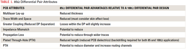
During high-speed signal propagation, the signal predominantly travels along the conductor surface. A conductor’s surface roughness contributes to signal degradation. The total signal loss is the combination of the losses by the conductor and dielectric laminate. Since laminate or dielectric loss increases proportional with an increasing frequency, and the conductor loss is proportional to square root of the frequency, trace surface texture and width exhibits a smaller contribution to signal degradation. An 85Ω design having reduced trace width and laminate thickness, favorable electrodeposition within a plated through-hole, the potential to employ small diameter PTHs, acceptable production yields, and lower board fabrication complexity offers conceivable cost savings and improved fabrication predictability.
High-speed connectors often have finished PTH nominal diameters ranging from 0.46 to 0.60mm and, in accordance with RoHS, will have PTH finishes other than SnPb. These finishes may include immersion tin or electroless NiAu and require PTH tolerances often more stringent than those associated with SnPb finishes. Successful electrodeposition within these PTH holes depends on the fabricator’s technical expertise and is gated by the multilayer nominal thickness ratio to the finished PTH diameter. Reduced PCB thickness contributes to minimizing this ratio and promotes uniform metallization of the PTH wall and robust connection to innerlayer traces. Figure 1 depicts uniform PTH geometry and innerlayer connections.
Laminate material intrinsic properties, dissipation factor or loss tangent, Df and dielectric constant, Dk, PCB process stability, and transmission clarity define the end-product performance and predictable conformance to requirements. A technically competent backplane supplier has a relationship with the PCB supplier who has characterized the signal integrity variables, including the effective dielectric constant, Dkeff. The Dkeff accounts for the influence of the combined core and B-stage laminate upon impedance and signal propagation. There should be demonstrable process capabilities supporting composite construction, sequential lamination, back-drilling, and finishes providing RoHS compliance and long-term reliability.
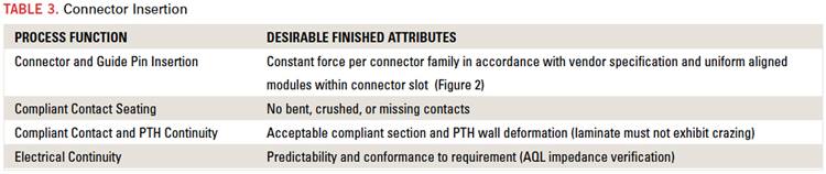
Having selected a prototype and production supplier that has foregone technical capabilities, comprehensive process predictability, conformance to requirements and consistency must be demonstrated through effective monitoring and statistical process control. This includes the fabrication process, assembly process, and the finished product’s electrical and mechanical performance. These process and finished product attributes have been tabulated in Tables 2 and 3.
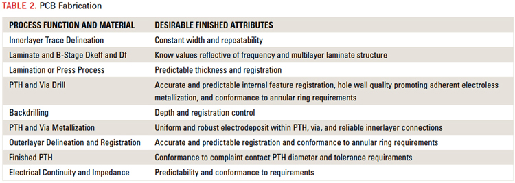
Many of the process functions shown in Tables 2 and 3 may be continuously monitored and predictability verified through the application of SPC, specifically
control charts depicting upper and lower limits that conform to the unpopulated and populated backplane’s physical and electrical requirements. In addition to control charts, the process capability index should be known. Several companies have developed automated finished production monitoring test equipment applicable to the unpopulated and populated backplanes. Capabilities include measurements defining impedance, propagation delay, effective dielectric
constant, S parameters, and verification of compliant contact seating.
When selecting a backplane manufacturing source, be it for prototypes, production or both, the following criteria summarize the material and technical function and backplane verification promoting efficient transition from design to viable hardware:
- Demonstrated SPC, including incoming material, fabrication and electrical test, continuity and impedance.
- Competent process control through the assembly operation employing control.
- Charts reflective of compliant insertion parameters, x-ray verification and assembled electrical test.
- Populated backplane electrical test beyond continuity to include impedance and S parameters. AQL may be applied to impedance and S parameter verification.
High-speed backplane fabrication and assembly meeting technical, price, and delivery requirements is readily achievable when a connector system is selected through knowledge of PCB fabrication and a thorough understanding of the required performance attributes and their applicability to system performance. Stringent and comprehensive quality control procedures drive cost efficiencies, on-time delivery, and consistent performance solutions.
Carl Hornig, P.E., is a consulting engineer and former technical director backplane fabrication, signal integrity, and assembly at Sanmina (sanmina.com); This email address is being protected from spambots. You need JavaScript enabled to view it..


