Neck-downs and vias are common “choke points” for current, but there are design solutions.
PCBs get hot. This is especially true of modern PCBs, packed with power-hungry ICs dissipating more heat than ever. But heat generated by the ICs isn’t the only consequence of their thirst for amps. The power distribution network, or PDN, must be designed to provide adequate DC current-carrying capability; otherwise additional heat can be generated on the board itself.
It is difficult to design a PDN that meets the high current demands of today’s ICs. Not only has the amount of current increased, but so has the number of different voltages used by the ICs. This means that power planes have to be segmented into multiple different islands, and trying to piece together all those different islands can often lead to neck-downs in the plane shapes. Additionally, lower voltages are being used – some less than 1V – which means there is very little margin for any voltage to be lost due to resistance in the PDN. And, of course, there is pressure to lower PCB costs, which limits the number of plane layers used in a design.
Common problems associated with inadequately designed PDNs include voltage drop, excessive current in vias, and excessive current densities in some area of the board. Drops in voltage can result in insufficient voltage at the IC power pins, which can lead to IC malfunction. Excessive current densities can lead to board damage and disconnected power in extreme cases, but will also result in board heating. Heating of the board by the PDN contributes to the overall heating problem on the board, and can reduce IC life.
These types of issues can be pinpointed and eliminated during the design phase through the use of analysis tools. One of the types of power integrity simulations performed is a DC drop analysis, or IR drop analysis, so named because it simulates the drop in DC voltage caused by current (I) traveling through the resistance (R) of the planes. Power planes can be mapped out in the pre-layout stage, or completed PCB designs can be analyzed to pinpoint possible neck-down areas, such as the area shown in Figure 1.

Such areas of high current density need to be eliminated, and these areas aren’t confined to neck-downs in the planes. Vias are another common “choke point” for current. Knowing how many vias to use to transfer power from one layer to another, or to connect a voltage regulator module (VRM) to the rest of the circuit, is not always intuitive.
Thermal analysis. It is also not straightforward to extrapolate temperature rise from a given current density. Many variables affect how the heat will dissipate, and the resulting temperature rise for that location. For instance, the method of connection of the “hot spot” to the rest of the plane is a large factor. Copper conducts temperature, not just electricity. Also, the percentage of metal in the surrounding layers above and below this area, as well as the board environment, will affect the temperature. These are the types of factors included in a thermal analysis. By performing a thermal/IR drop co-simulation, these hot spots in the planes can be examined for precisely how hot they will get.
Thermal simulations model all three methods of heat transfer: conduction, radiation and convection. Heat is conducted from the ICs through their pins and then throughout the board. Heat is radiated from the ICs and from the board. Heat is also transferred through convection – naturally, opposite the direction of gravity, as well as through forced convection if there is some type of fan or blower in the system. When a high current density area exists in a PDN, it acts like another heat source, and that heat gets dissipated by a combination of these three methods of heat transfer.
Voltage drop and temperature are actually closely related, because the resistance of copper changes with temperature. In fact, copper conductivity changes 4% for every 10˚C of temperature change. A temperature range of 80˚ equates to a 32% change in copper conductivity, which is quite significant. As such, to determine the actual current densities in the copper on the board, the temperature of the board must be known. And in order to determine the temperature on the board, the current densities on the board must be known. Hence, there is a need for a co-simulation between IR drop and thermal analysis in order to generate accurate results.
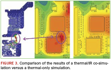
So, to accurately predict the temperature rise caused by areas of high current density, the temperature of the board must first be known. This requires, at the very least, modeling the power dissipation of the components, their connection to the board, the board itself, and the environment the board is in. With this information, thermal simulation can be used to develop a thermal profile of the board, which can then be fed into an IR drop simulation to ensure the appropriate copper conductivity. The results of the IR drop simulation can then be fed back into the thermal simulation to include the effects of power being dissipated by the PDN, and this back-and-forth iteration of simulations can continue until the simulators converge on a solution. An example of such a simulation is shown in Figure 2.

This simulation includes the heating effects of a 1.5V plane that is feeding two larger ICs on the right side of the board. Thermal effects are a little different from electrical effects in that it is much more difficult to isolate them. Electrical effects can be examined on a per-net basis. For example, a single signal net can be examined for signal integrity, or a single power net can be examined for power integrity. In thermal analysis, the entire board, including its environment, needs to be analyzed at once. As such, for maximum accuracy, all the power nets on the board, including the ground net(s), should be analyzed at once, since they all interact.
In this example, more clearly depicted in Figure 3, there is obviously an area of increased temperature on the board corresponding to the area of high current density on the plane. Comparison against a thermal-only simulation reveals the importance of including the heating effects of the PDN.

More important, the heating effect of that plane shape neck-down is accurately characterized, and provides valuable information in driving a design change on the board. In this instance, the easiest solution would be to eliminate that neck-down on the plane shape. However, if that plane is feeding multiple voltages throughout the board, that may be difficult. Another solution may be to add another shape on another layer to help “bridge” the gap where the neck-down occurs, and stitch it to the existing plane shape using vias. Such a fix could be analyzed by performing another simulation.
Other hotspots. It is important to note that such plane shape neck-downs aren’t the only PDN design issues that can cause thermal problems. On any design with BGAs, especially finer-pitch BGAs, such problems will naturally occur in the breakout area beneath the BGA. There, the power planes are often perforated with antipads from signal and ground vias, forming a narrow web of copper to feed current to the power pins. These areas are commonly areas of very high current density, which can cause the same type of heating issues (Figure 4).

These areas can be especially problematic because they are already the highest temperature areas on the board, because they reside beneath the ICs. The ICs are typically the most significant sources of heat on the board, and the areas beneath them tend to be the hottest areas on the board as a result. Adding additional sources of heat to these areas – areas of high current densities caused by perforated planes – leads to higher temperatures on the IC and ultimately reduced component lifespan. For every 10˚ above 100, the mean time between failure (MTBF) of a component is reduced by as much as 50%.
Power pins and stitching vias can be another area of the design at risk for thermal issues. It is important that any VRM attached to the power planes be attached with adequate power pins and/or stitching vias, so that the current is distributed and temperatures of those pins and vias are kept relatively low. The same is true for vias stitching multiple power planes together.
Thermal issues are often solved in a variety of ways: adding heatsinks to components, changing airflow, or separating hotter components, to name a few. Thermal issues caused by inadequate PDN design have one simple solution: add more metal. This may mean widening traces carrying significant current, eliminating neck-downs from plane shapes, using thicker copper on the planes, or adding more stitching vias where necessary. The solution is simple. Through analysis of the power distribution system prior to building the boards, such problems can be quickly identified and resolved. This will result in designs that are more reliable and last a long time.
Patrick Carrier is product manager, high-speed PCB analysis tools, Mentor Graphics (mentor.com); This email address is being protected from spambots. You need JavaScript enabled to view it..


