 The loss of x-axis and y-axis flexing can increase the stress to internal interconnections.
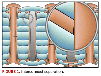
Thermal cycle testing analyzes how interconnections fail and what the contributing factors are to those failures. Interconnect separation can be described as a separation between the copper foil on an internal layer and the copper in the barrel of a plated through hole (PTH). Interconnections are typically robust and do not fail in thermal cycle testing, but if the interconnection is weak, a crack can develop between the foil and the barrel of the PTH.
Stress is applied to the interconnect structure due to the z-axis expansion of the dielectric during thermal excursions. There is significant z-axis expansion associated with assembly and rework, and significant thermal excursions are experienced with tin/lead reflow, fusing and hot-air solder leveling (HASL). Other sources of thermal excursions include lamination and baking cycles.
As the dielectric around the barrel of the hole expands, the PTH acts like a rivet that resists the expansion. The connection of the pad to the barrel of the hole effectively locks the interconnection in place while the outer edge of the pad is free to move with the dielectric material. The result is a condition called pad rotation.
The degree of pad rotation increases from the middle of the printed circuit board (PCB), which experiences no rotation, to a maximum deflection at the upper and lower surfaces. The greatest deformation of the internal interconnection occurs on layer 2 and layer N-1. Dielectric material with a higher coefficient of thermal expansion (CTE) invokes a greater pad rotation. Materials with a lower glass transition temperature result in the onset of higher expansion rates at temperatures lower than materials having high Tg. The thicker the board and the higher the resin content, the greater the pad rotation will be.
Grid size plays a role in pad rotation. Larger grid sizes (0.050 inch or greater) allow a greater amount of expansion of the dielectric between PTHs during thermal excursions. Smaller grid sizes tend to constrain material expansion between PTHs, thus reducing the amount of the dielectric that can stress relieve by squeezing out between PTHs during thermal excursions. Materials with a lower viscosity can expand between PTHs, invoking pad rotation, while materials with a high viscosity will be constrained by PTHs and induce a lower degree of pad rotation.
Holes that are rough due to drilling or aggressive desmear seem to increase stress at internal interconnections. It appears that a rough hole is very rigid and inflexible, resisting the inward compression due to x-axis and y-axis expansion. A printed through hole with a rough hole has a configuration that is similar to a corrugated can, with the ridges resisting compression at the PTH’s side walls. The loss of x-axis and y-axis flexing appears to increase the stress to internal interconnections. Surface finishes with nickel tend to strengthen the PTH, increasing the propensity for interconnect separation. Larger holes also seem to resist compression and to increase stress at internal interconnections.
Interconnect separation is usually expressed as a crack that propagates at the internal interconnection. The crack is wedge-shaped, with the large end on the side of the foil closest to the middle of the PCB. An interconnect failure frequently develops slowly, accumulating damage at a constant rate after onset. Constant damage accumulation can be seen in the resistance graph, FIGURE 1.

An elastic dielectric material will return to its original shape between thermal excursions, and one can imagine that a developing interconnection crack could close between thermal excursions. As the dielectric returns to its original shape, the crack closes and the resistance at the failing interconnection drops. This return to the original resistance between thermal excursions is analogous to self healing. As material ages, elasticity is reduced and the dielectric may undergo plastic deformation during thermal excursions. If the crack at the interface is held open between thermal excursions, due to plastic deformation of the material, a resistance hysteresis may be observed. If pad rotation is observed, material deformation is inferred – given that a microsection is processed on the PCB at an ambient temperature.
Paul Reid is program coordinator at PWB Interconnect Solutions Inc.; This email address is being protected from spambots. You need JavaScript enabled to view it..


 The loss of x-axis and y-axis flexing can increase the stress to internal interconnections.


