Over time, the feedback loop of testing, adjusting and retesting can significantly improve PCB reliability.
A PCB’s reliability may be evaluated using thermal cycling. Thermal cycle testing to failure allows an objective estimation of reliability, and testing is usually performed at elevated temperatures – ones that are higher than the end-use environment. This provides a practical method that produces timely results, allowing one to assess relative reliability. Testing may be performed on representative coupons that have the same configuration as the PCBs. By convention, testing continues until either the end of test or a failure, which for the data used to produce these columns, was a 10% increase in resistance in any test circuit.
Thermal cycle testing establishes relative reliability. Coupons that have been fabricated poorly, for example, coupons with thin copper plating in the barrel of a plated through-hole (PTH), will survive fewer cycles than coupons with adequate copper plating. Once failures occur, microsections can be processed so that the specific failure mode can be analyzed.
Thermal cycle failures include failures of either the copper interconnections or the dielectric material used. Understanding how they fail can give insight into the root cause. Once a failure mode and cause is understood, steps can be taken to improve PCB reliability, and changes can then be adopted. The relative improvements in the process can be objectively tested, providing a feedback mechanism for continuous improvement. This feedback loop of testing, adjusting and retesting is a very powerful tool with the potential to significantly improve PCB reliability over time, translating into improved yields and reduced cost.
Armed with an understanding of PCB fabrication, microscopic examination of failure sites allows one to establish a probable cause for failure, and at times, the cause of failure is obvious. It is not hard to understand that thin copper in the barrel of the PTH is a reliability liability. At other times, determining the cause of failure is difficult. For example, it is difficult to directly view detrimental changes in a material’s visco-elastic properties using light microscopy, due to the thermal excursion of assembly and rework. Frequently, the ways PCBs fail are due to the influences of a number of factors, not all of which are visible in a static microscopic examination.
Microsections are processed on a sample that has been cooled to an ambient temperature. This is a static view of a dynamic process that was occurring as a result of thermal cycling. Microsections are snapshots in time of a failure that has been evolving or maturing. To better understand how failures form and develop during thermal excursions, the digital edition of this issue will contain a series of animation of the failure. These animations are based on the examination of thousands of microsections, thermal mechanical analysis, thermal cycling data and plotting increases in resistance of failing circuits during thermal cycling and illustrate how types of failures may develop. These animations are not to be considered accurate in scale but rather an artistic rendering, with key features enhanced to improve understanding of various failure modes. For expediency, the animations demonstrate, in one or two thermal cycles, the accumulated damage that may occur over hundreds of thermal excursions.
The first animation,
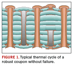
FIGURE 1, represents a typical thermal cycle of a robust coupon that does not fail. It serves to establish the relative effect of a thermal excursion on a PCB heated to assembly temperatures. Notice that the dielectric material expands from the middle of the board, and the degree of material displacement increases from the middle of the board outward, with the maximum expansion occurring at the surface layers. The PTH structures act like small rivets constraining the z-axis expansion of the dielectric material, with the dielectric bulging out between the constraining PTHs. The coefficient of thermal expansion (CTE) of the dielectric material is usually an order of magnitude larger than the CTE of the copper. This mismatch between the CTE of the dielectric material and the copper creates significant stress in the PCB, and it is the primary cause interconnection failures.
 View an animated version of Figure 1
Note that the copper is malleable and complies with the expanding dielectric material. The PTH exhibits a slight inward bow during the thermal expansion, as the compressive forces on the x-axis and y-axis deform the copper barrel inward. The pad rotation on the PTH and buried vias is away from the middle of the PCB. The microvia, floating between the PTHs, has a pad rotation toward the middle of the PCB. The buried vias exhibit a deformation that is localized and of a lesser magnitude than the adjacent PTH, based on its lower position in the structure. The PTHs, buried vias and microvias all influence the deformation of the material that is in close proximity and on adjacent structures.
PCD&F
Paul Reid is program coordinator at PWB Interconnect Solutions Inc.;
This email address is being protected from spambots. You need JavaScript enabled to view it..


