Good drilling and registration are critical to the success of microwave designs because embedded filters and couplers can be adversely affected by poor hole quality and misregistration.
PTFE containing composites offer the promise of exceptional electrical benefits at high frequency. However, this attraction to PTFE is soured by some manufacturers’ vision of the fabrication challenges. Mechanical drilling and registration are two key areas that fabricators struggle with when fabricating high layer count products. These learning curve hurdles can be greatly reduced by understanding some key processing variables. Recent introductions of non-reinforced PTFE prepregs and dimensionally stable cores offer the promise of building 250-mil to 300-mil large format PCBs with the same quality and predictability as FR-4. However, the attractiveness of isotropic, electrically homogeneous fiberglass-free dielectrics is diminished by some fabricators’ lack of experience with PCBs containing PTFE and little or no fiberglass.
While fiberglass-rich PTFE composites might be more dimensionally stable, fiberglass suffers from the following drawbacks: high 0.0067 Df at 10 GHz that becomes increasingly worse with frequency plus the problem that fiberglass is very anisotropic at the millimeter/micron level.
Publications highlighting the drawbacks of using fiberglass-based laminates in multilayer stripline applications are numerous. Various authors1 have shown the high level of impedance variation that can be observed by time domain reflectometry (TDR), as a transmission line crosses between the windows and knuckles of woven fiberglass. Loyer
2 has shown that while there might be an average skew number, depending on how the transmission lines are routed on a typical FR-4-based PCB, there is a distribution of skew that will occur on a fiberglass-reinforced FR-4 composite such that some transmission lines can be much better or worse than others.
2 The ideal case is a fiberglass-poor stripline structure. A PCB with excellent electrical properties that cannot be manufactured with high yields and predictability is of no use to the industry.
Designers generally accept the claims of the exceptional electrical properties of ceramics, like silica, and thermoplastics, like PTFE.3 During testing of a series of PTFE containing prepregs and cores, a great deal of emphasis was placed on working with high volume, large format, backpanel manufacturers to understand the mechanical drilling of composites containing some level of PTFE. The goal was to improve the quality of the drilled hole, particularly with respect to plating nodules. Some OEMs do allow 1-mil to 2-mil nodule in their specifications, while others see any nodule as a potential risk to long-term reliability. While not all PCB applications have the concern that a plating nodule might damage a press fit connector, the plating of poorly drilled via structures can lead to shorts or opens. In digital applications, at high frequency, the vias and ground vias are highly tuned with respect to capacitance/inductance so that the via itself provides a smooth 50-ohm or 100-ohm transition without a high level of return loss/insertion loss roll off. In a microwave application, one worries that copper-plated debris in a through-hole can significantly degrade filter or coupler performance. The installed FR-4 base of fabricators and suppliers have experience drilling FR-4 and have optimized their processes around it. Today’s ceramic-loaded PTFE composites have been optimized for reduced expansion/contraction, and insensitivity of Dk and Df to temperature, frequency and moisture. Improvements have been made to PTFE materials to yield more homogeneous composites that are easier to drill and to plate. Fabricators must still take the time to understand what is being fabricated.
First, a basic strategy to mechanically drill standard ceramic-loaded PTFE laminates will be presented.
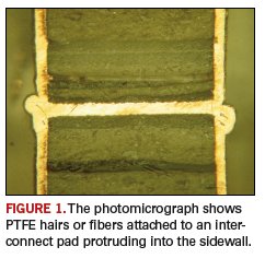
FIGURE 1 shows what looks to be PTFE hairs attached to an interconnect pad. This defect is a common problem encountered by fabricators and often leads to plating nodules. Secondly, the defect raises questions about long-term reliability. An 18-layer, 165-mil backpanel board produced with one-ounce copper was cross-sectioned, carbon coated and analyzed using a JEOL 5300 Scanning Electron Microscope. The JEOL 5330 used voltages of 20 kV to 25 kV in combination with a Kevex SiLi detector that used backscattered electrons in either the compositional or topographical models. Typically, copper generates a series of three KeV peaks. Because an electron beam causes a cascading effect of excited secondary electrons and x-rays, 4 microns to 6 microns is the typical beam resolution. Therefore, neighboring copper is typically included in many EDX scans. SEM/EDX was used to analyze a plating nodule occurring at an interconnect pad.
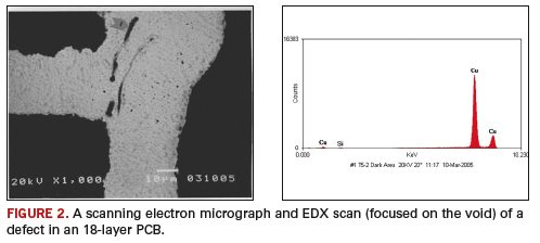
FIGURE 2 is interesting because the low energy copper KeV peak has disappeared in the EDX scan. The electron beam was focused directly into the black area in Figure 2. This suggests that the low energy back-scattered copper electrons have disappeared, which is consistent with focusing the electron beam into a deep void. Figures 1 and 2, combined with exhaustive analysis of similar defects, strongly suggests that the “hairs” are actually voids. What is the source of these voids?


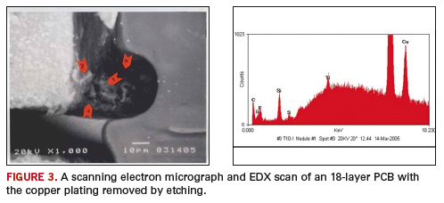
The 18-layer PCB samples were potted, and the plated copper was etched out of the sidewall leaving the bare hole wall, associated debris and the potting compound still in place.
FIGURE 3 shows the multilayer PCB after the was sectioned and the plating removed. The interconnect pad can also be seen to have been removed during etching. Directly above, where the interconnect pad had been located, is a loose collection of bound particles. EDX shows PTFE, titanium dioxide and silica. The fact that the loosely associated group of particles rests just above the interconnect pad strongly suggests that the dominant mechanism causing these defects is the interconnect pad scraping drill bit debris off the bit as the bit enters and exits. After thoroughly analyzing other areas showing the same defect as Figures 1 and 2, the evidence is compelling that the mechanism resulting in these hair-like voids and nodules is debris that builds up onto the drill bit and scrapes off onto the sidewall when the bit hits a copper interconnect pad. This loosely associated lint-like collection of particulate then challenges the plating process. Electroless and electrolytic plating chemistries try to plate in and around the random collection of debris that is attached to the sidewall, leaving plating voids.

Drilling is a dynamic process. Material is reduced in size to particulates, with the hope that the debris will move up the flutes and will be evacuated by the vacuum system.
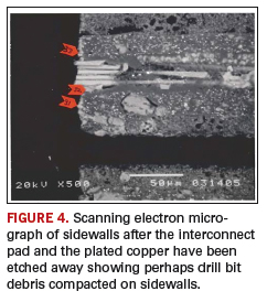
FIGURE 4 shows an SEM scan of a sidewall, where no defects can be observed. However, drill bit debris can be seen lining the sides of the hole walls. When one uses scanning electron microscopy to look very closely at hundreds of holes after etching away the copper, one is likely to see defects that are normally plated over and embedded into the copper.
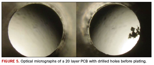
FIGURE 5 shows a good via versus a bad via before plating. High-pressure washing may loosen attached debris from the hole walls, but it won’t remove debris that is fused to the sidewall by hot PTFE.


There are many variables to consider when drilling printed circuit boards, including entry materials, exit materials, drill rpm, infeeds, chip loads, hit count, primary angle of the drill bit, drill type and retract rate. The secret to drilling PTFE is not to allow debris to build up on the surface of the drill bit. PTFE is a soft material, and as PTFE gets hot, it acts as a binder and glues the debris to the flutes of the bit. As the drill bit burrows the hole, it strikes the copper interconnect pad. Debris scrapes off the bit and is deposited on the interconnect pad. Drill bit debris cannot be allowed to build up on the bit – but how do you accomplish this? The variables to be considered included:
- Drilling with a low chip load and at low speeds
- Drilling using a thick, hard phenolic entry material
- Inserting a dwell time between hits to cool the drill bit
Good drilling parameters should allow no debris to accumulate in the flutes of the bit. Drill bit debris can be removed by drilling the contaminated bit into a hard material like phenolic. The objective is to abrade the debris onto the hard sacrificial entry material. One DOE began by drilling twenty 0.0028-inch holes into a 200-mil thick, ceramic-filled PTFE multilayer PCB. The PCB was removed from the drill table and replaced by a 160-mil slab of phenolic. Drill bits full of debris were drilled 20 hits into the phenolic and examined. The hard phenolic effectively abraded the debris off the bit, cleaning it. The bits were alternately drilled 20 hits into the PCB and 20 hits into the phenolic, reaching 200 hits into the PCB and 200 hits into the phenolic. This experiment demonstrated that through 200 hits, the drill bit could be effectively cleaned of PTFE debris by using hard phenolic to abrade the PTFE off onto the phenolic. Although phenolic may not be the best entry material, it performed better than using FR-4 as an entry material. It is postulated that a harder phenolic may work better.
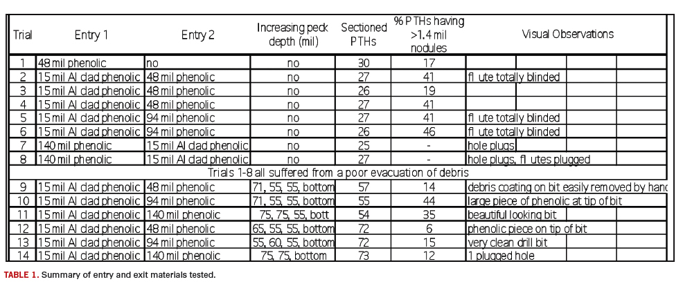
However, removing a backpanel-sized PCB from the drill table and alternating with a phenolic dummy every twenty hits is not a practical manufacturing solution. The next experiment used a thick piece of phenolic as the entry material to essentially clean the drill bit every hit, as opposed to waiting for 20 hits and allowing debris to build up on the bit. The largest unknown was how thick the phenolic entry should be to effectively abrade all of the debris off the bit before it began to drill into the 200-mil thick, ceramic-filled PTFE PCB. A 200-mil thick, 20-layer, ceramic-filled, PTFE-based PCB was drilled with the following parameters: 32 K speed, 48 K infeed, chip load = 1.5, 1 second dwell between hits, 28-mil diameter straight shank Kemmer bit, retract rate 1000 and 70-mil phenolic exit material. The entry and exit materials are summarized in
TABLE 1.

Trials 1 through 14 show the use of various thicknesses of phenolic entry material to essentially abrade the PTFE debris from the bit before it could drill into the PTFE-based PCB. A variety of thicknesses of phenolic entry material was used, including 48 mil, 94 mil and 140 mil. Trials 1 through 8 highlight the use of thick phenolic entry with no peck drilling. The problem with using thick phenolic entry material is the difficulty in evacuating all the phenolic debris, which is a new variable. Trials 5 through 8 used 94-mil and 140-mil phenolic entry and resulted in drill bits and hole plugs inundated with phenolic. In the absence of peck drilling, only Trials 1 through 4 had some hope of success using the thinner 48-mil thick phenolic. Trials 9 through 14 took advantage of peck drilling to remove debris more effectively. As shown in Table 1, the trials using the 48-mil phenolic entry outperformed the trials using the 94-mil and 140-mil thick phenolic entry. Although the thicker phenolic entry is more effective at cleaning the PTFE-based debris off the bit, the phenolic entry itself becomes difficult to remove during drilling. Trials 9 and 12 are interesting because they use the same drill conditions with the only modification being the peck depth. Trial 12 yielded the best results when the first peck drilled to a depth of 65 mils (48-mil phenolic + 15 mil Al-clad phenolic) effectively only traveling to the depth of the phenolic to clean the bit, then retracting to remove debris associated with the phenolic. This yields a penetration of only 1 mil to 2 mils into the PCB before the debris is evacuated and the cleaned drill bit is free to start drilling a single hole in the PCB. In Trial 12, the first peck traveled 65 mils, barely passing beyond the entry materials into the PCB, the second peck drilled an additional 55 mils (total depth of 120 mils) before retracting, the third peck traveled an additional 55 mils (175 mil depth) and the final peck drilled to the bottom of the PCB.
There are a lot of variables in the mechanical drilling process, and future experiments should focus on the optimum thickness of phenolic entry to balance bit cleaning and phenolic evacuation, phenolic hardness and optimum pecking.
Another variable investigated was the dwell time between hits, used conceptually to allow the bit to cool. Normally, PCB fabricators drill at the maximum possible speeds to achieve the highest possible utilization of the drill machines, using nanosecond dwell times between hits. A similar experiment was conducted with a standard 10-mil phenolic entry material to look at the dwell times between hits. The dwell time was varied from 0.04 seconds to 8 seconds and no peck drilling was used. The short conclusion is that the trial with a dwell time of 0.04 seconds between hits had three times more nodules then the trials that used a range of 1 second to 8 seconds as the dwell time. There was no apparent advantage in using longer than 1 second. This experiment was conducted prior to the DOE conducted in Table 1, so it is quite possible that the peck drilling may be sufficient to allow the bit to cool without a dwell time between hits. A one-second dwell might also prove no better than 0.5 seconds or 0.25 seconds.
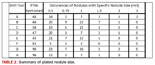
A further study was conducted specifically on 10-mil drilled holes to compare the drill quality of different geometries. Smaller bits, 8-mil, 10-mil and 12-mil, raised the level of complexity. Small bits are more prone to breakage, and they are much more susceptible to drill wander. Because small bits are more prone to breakage, one has to balance the thickness of the phenolic entry versus the increased level of breakage that occurs with a longer, fragile drill bit. Small bits will deflect off hard materials in the composite, causing wander. Drill wander is another level of complexity that challenges registration of innerlayers above and beyond the dimensional stability of the innerlayers during fabrication. The following drill parameters were used, and all held constant: entry material (7 mil Al, 16.5 mil phenolic entry), exit material (16.5 mil phenolic), infeed (55 ipm) and speed (120K rpm). This set of drill conditions was previously found to be a solid set of drill parameters for 10-mil holes. Four drill bit vendors were evaluated, and both undercut and straight shank bits with various helix angles were evaluated. Typically, thicker phenolic entry would be preferred for better removal of debris from the drill bits. Regrettably, not all vendors could supply drill tools of sufficient length to allow for thicker phenolic entry material. The ceramic-filled PTFE substrate material was approximately 115 mils thick and had 1 ounce copper planes every 10 mils. The drilled holes were then visually evaluated before plating, metalized, and reevaluated by tedious cross sectioning. Nodules in the plated through-holes (PTHs) were counted and ascribed to a certain size (mil) so that a size distribution of plated nodules could be obtained. The plated nodule size distribution is summarized in
TABLE 2.

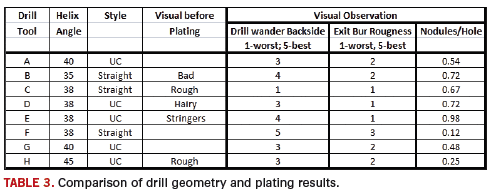
From this crude analysis, drill tools F and H showed the least amount of plating nodules and the smallest number of large nodules relative to the number of 10 mil holes cross-sectioned. The drill geometries are summarized in
TABLE 3. In an attempt to attach a score to the relative roughness of the hole corresponding to each drill condition, Table 3 contains a category listed as “the number of nodules divided by the 10 mils cross-sectioned.” From this scoring, drill tools F and H showed the best results.

Drill tool F was a straight shank tool, and drill tool H was an undercut bit with an unusual 45â—¦ helix angle. Contrary to popular thought, undercut bits did not show any advantages versus a straight shank tool using this set of drilling conditions. A standard straight shank drill tool outperformed all candidates. In fact, drill tools E and F were from the same vendor, with this vendor’s undercut tool being the worst candidate and their straight shank tool being the best.
The backside of the test substrate was also evaluated visually for drill wander. Generally speaking, the best drill parameters may not correspond to the least amount of drill wander, so a set of drill conditions must be adopted that balances an acceptable level of drill wander with acceptable hole wall quality. Small diameter drill bits are particularly prone to wander when drilling high aspect ratio through holes. Again, drill tool F outperformed the other drill geometries, having the least amount of drill wander. Because the drill parameters were fairly well optimized, the bits showed no sign of the flutes being filled with debris. Bits that have flutes full of PTFE and related debris are even worse from a drill wander perspective. With good processing parameters, 20-layer to 30-layer, 150-mil to 275-mil thick multilayers are being fabricated in a predictable fashion, with virtually no fiberglass reinforcement.
Many people understand that high quality PTHs are preferred from a reliability viewpoint. However, for microwave designs, where designers are embedding filters or couplers inside a PCB, through hole quality is essential. If a PTH is used in the design of filters or couplers and random debris occurs on the interconnect pad, this has the possibility of influencing the capacitance/inductance of the circuit and being detrimental to the performance of the filter/coupler. Poor registration can also affect the performance of a filter embedded in a multilayer design. Registration is a challenge that has its roots in the performance of the core materials. If a core material is poor at maintaining registration, then the problem is exacerbated by drill wander. Taken together, registration and plating debris (nodules) are serious problems for the filter and coupler designer.
Designs incorporating 0.4-mm and 0.5-mm pitch are becoming standard in the semiconductor test area. This trend corresponds to the use of smaller drill bits. The trend in microprocessors is obtaining a higher I/O count, meaning there is a pressure on densification in the semiconductor test area. Thousands of I/Os make it essential that the PCB supplier takes the time to understand all of the factors that lead to poor drilling and poor registration.
PCD&FREFERENCES
Lee Richie, “Impact of Glass Weave on Skew and Jitter,” copyright Speeding Edge, February 13th, 2007.
Jeff Loyer; Richard Kunze, and Xiaoning Ye, “Fiber Weave Effect: Practical Impact Analysis and Mitigation Strategies,” IEC DesignCon 2007.
Heidi Barnes, Jose Moreira, Thomas McCarthy, William Burns, Cresencio Gutierrez, Mike Resso, “ATE Interconnect Performance to 43 Gbps using Advanced PCB Materials,” IEC DesignCon 2008.
Thomas F. McCarthy is VP advanced technology and business development at Taconic and can be reached at
This email address is being protected from spambots. You need JavaScript enabled to view it.. Oliver Zhu is a field technical manager at Taconic and can be reached at
This email address is being protected from spambots. You need JavaScript enabled to view it.. Anthony Serafino is a process engineer at R&D Circuits and can be reached at
This email address is being protected from spambots. You need JavaScript enabled to view it.. Brigitte Lawrence is owner and president of Brigitflex, Inc. and can be reached at
This email address is being protected from spambots. You need JavaScript enabled to view it..


