DC simulations can help meet tight voltage margins and avoid field failure risk.
The power handling capacity for IC package and printed circuit board structures is a major design challenge and a critical factor for successful product implementation. The trend to pack more performance onto chips has necessitated operating with higher current at lower voltage levels. Under- and over-voltage conditions impact end-product performance and reliability, making DC analysis an important requirement for PCB and package design flows.
Supplying a constant two volts to a chip was fairly straightforward when the required current was 40 amps, but those days are long gone. Today, voltage tolerances are razor thin challenging designers to meet 5% or less of nominal operating voltage.
Marketplace realities exacerbate the challenge. Those with tight schedules, fixed end product price points and constrained physical dimensions can not simply add copper and layers. Going forward, difficulties will only increase.
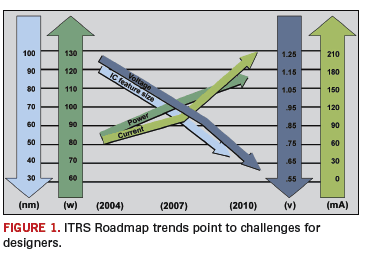
As seen in FIGURE 1, clock rates and current loads are rising at the same time chip voltage levels and feature sizes are declining. The International Technology Roadmap for Semiconductors (ITRS)1 points to challenges across diverse chip product lines from high-end microprocessor to consumer portable devices. While the pressure for processing speed will accelerate, there is an upper bound on available power. On-chip Data Processing Engines (DPEs) have rising power appetites that can outstrip package sourcing and dissipation limits, and mobile devices are limited by the imperative to conserve battery life. According to the ITRS Roadmap, current package power limits will be exceeded by 4x by 2020, resulting in a forced reduction of chip content and logic activity.

IR Drop
Delivering reliable power to circuits is always of critical importance because DC drops can happen at every level in a chip, package and board system.2 Components that are distant from their associated power source are particularly susceptible to IR drop, and designs that rely on battery power must minimize voltage drop to avoid unacceptable power loss.
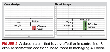
From a board design point of view, component supplier datasheets provide a valuable reference and guide for the total margin of both DC IR drop and AC noise. For the end product to function as anticipated, power fluctuations must remain within datasheet tolerances. Traditionally, design teams have used a ratio of 80:20 for AC noise / IR drop. The higher percentage of the margin allocated for AC is necessary because issues associated with noise can be particularly difficult to mitigate. Still, the resulting squeeze on the DC budget increases the headaches associated with assuring overall power efficiency, reliability and performance. The good news is that when designers pay close attention to DC performance, they are rewarded with an additional cushion for managing AC noise, as depicted in FIGURE 2.

Basic DC Analysis
Early DC assessments help determine power distribution basics such as the best available entry point for power, layer stack-up choices and estimates for the amount of copper needed to carry the current. A design team may anticipate a processor will draw 80 amps to 100 amps, and the design will require six routing layers. Traditionally, voltage drop analysis for a design like this utilized spreadsheet estimations that considered resistivity for simplified geometry profiles. For simple designs with uniform plane shapes and a single voltage to consider, this can be sufficient if the margin is ample.
Things get much more complicated, however, for designs with multiple sinks, various voltage levels and irregular plane shapes. Further, spreadsheets cannot perform important via current calculations, and beyond this, it is a rare design team that finds itself with margin to spare. Designs with 10 or more unique power domains almost always require splitting power planes, and, many times, there is a need for copper area fills on signal layers, which adds to the complexity. In cases like this, spreadsheet-based calculations fall short and generate a false sense of security.
DC Simulation
Numerical DC analysis has emerged as a critical step in the design of high-performance packages and PCBs. Simulations determine if power nets are properly connected and confirm exactly how good the connections are. DC analysis tools go beyond spreadsheet calculations with accuracy that reduces the risk of field failure. Implemented early in the design cycle, these tools support planning and move with the product as layout proceeds.
Before detailed layout, DC analysis is useful for allocating budgets between the package and board. It can help determine the appropriate plane shapes and splits, where to position the multiple VRMs (voltage regulator module) and can identify preferred remote sense line locations. DC power distribution can strongly influence layer stackup. DC simulations enable design teams to produce the most robust system possible without wasting plane layers. Performing what-if assessments with various source and sink locations before routing begins enables design refinement while there is maximum flexibility.
The most advanced tools available today include adaptive triangular meshing to precisely model actual design geometries, including irregular shapes on every layer. This is critical to accurately simulate designs with via fields and planes that include arbitrary cuts, and simulation with a finite element engine tuned to DC analysis assures the most accurate results possible. Since most electronic products today are required to run close to targeted limits, accuracy is at a premium. Designs benefiting from very accurate DC analysis can yield downstream savings from reduced layer counts and the avoidance of expensive active cooling strategies where passive approaches suffice.
For large designs or multi-board simulations, analysis speed is an important issue. When simulations are tuned specifically to DC studies, run times are faster. A simulation tool optimized for DC calculations generally runs 3x to 10x faster than a general purpose AC / DC simulator. This enables the kind of rapid what-if assessment and design tuning needed for the best designs.
Quick DRC style pass / fail checks enable users to readily identify problems. Interactive what-if visualization is helpful in providing users with cues about insufficient power or excess current density. With this information, users can make adjustments to the design and confirm a robust implementation. Fast turn around enables physical layout tasks to continue unimpeded avoiding wasteful backtracking and rework.
VRM Tuning
Power supplies are linked to chips by a power delivery system that includes a VRM, printed circuit board and IC package. Where possible, VRMs are located on the same board as the loads, and generally, the VRM dominates performance up to about 100 KHz. Higher performance chips often include local VRMs. With effective DC analysis that considers nominal voltage levels and minimum input tolerances, sinks that are out-of-spec are quickly identified, and issues can be addressed by increasing VRM compensation.
VRM position, rotation and adjustment play a significant role in keeping designs within tolerances. Still, it can be tricky to understand how much the VRM nominal output voltage can be safely raised to maximize compensation. DC simulators are effectively used to assess design alternatives.
At times, users will want to define the ratio between the VRMs in a group to control current split. Similarly, some users may want to control their most complex power nets individually at selected chip locations. With more capable tools, sink location information can be further refined on a per-pin basis with values that are added through text files. Generally, this data comes from chip-level simulations. This per-pin information further refines the accuracy of multi-domain (chip / package / board) current estimates.
Remote Sense Line Location
Adding a remote VRM sense location plays a vital role in helping designers efficiently meet end-to-end voltage margins by detecting changes in loading and controlling voltage levels. If there is an increase in current, the VRM raises voltage output to compensate and to manage the additional IR drop.If the current is decreased, the voltage level similarly can be adjusted.
The location of the VRM remote sense line is critical for effective performance. Unfortunately, it is not always easy to identify the best location for a VRM remote sense, particularly when multiple devices are involved.
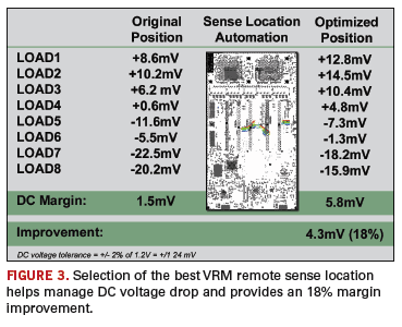
Having the sense located in the best possible position is critical, this single design optimization can increase the ability to meet targeted thresholds and significantly improve overall voltage margin efficiency by 10% to 20% compared to seemingly reasonable alternative locations. Even expert level power engineers find it difficult to pinpoint the best location using judgment and experience alone.
DC analysis tools can be extremely helpful in understanding the effectiveness of simulated remote sense location scenarios. As observed in FIGURE 3, recent breakthroughs also automate pinpointing the optimized location and avoid the need to iteratively simulate the myriad of possible implementations. Results for nearly every design show this one-step optimization approach significantly shaves DC margin.

Current Density Challenges
Accurately understanding plane current density can be a critical project success factor. Chip current requirements are so high that plane and via current density constraints must be carefully managed to avoid current distribution hot spots that introduce unnecessary thermal stress. Contributing to the challenge are higher component, via and routing densities combined with a desire to minimize layer counts and copper costs.
Current flow to components produces heat that must be transferred to surrounding structures efficiently, or component junction temperatures will rise, reducing product reliability. This possibility leads to a requirement that device junction and overall board temperatures are controlled to ensure they remain below specified limits. It also necessitates a comprehensive understanding of current density and the heat generated by the design’s current flow. Often, this is easier said than done.
In a design with thousands of vias, how do you find the one that will lead to field failure or identify which bumps and wirebonds are susceptible? The need to control current flow into vias is critical because high current density leads to temperature rise. It is very difficult to determine which via will fail, and beyond that, the failure of one via can trigger a cascade of via failures.
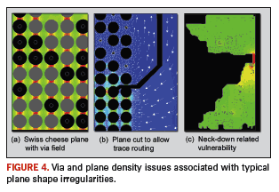
Swiss cheese via fields and unusual plane shapes (FIGURE 4) increase current density challenges, without careful analysis, this can lead to end-product reliability problems. Vias can act like fuses creating an overall system failure, and most designs include a few vias that exceed anticipated current limits. When failures occur, the cause is not immediately obvious even to expert eyes. While a designer may assume a neighboring plane will dissipate heat, planes with via fields will not have the anticipated effect. The risk is also high in areas where plane shapes neck-down or in areas with dynamic plane cuts. Excessive plane current density leads to thermal stress, dielectric failure and even fires in PCB organic substrates.

As design layout progresses, analysis can effectively identify risks. Areas in the design that neck-down contribute to excessive IR drop, and in cases where the neck-down area does not lead to an IR drop problem, thermal stress can be created. Sometimes this happens because of unusual cuts in plane structures for mounting holes and the like.
It is also typical that in the final stages of design, there is a need to route a signal net on a plane layer; these plane cuts impact current flow and lead to areas of excessive density. It is nearly impossible to avoid making some adjustment in plane layers as layout progresses, but by simulating them, issues can be quickly identified and mitigated without impeding design progress.
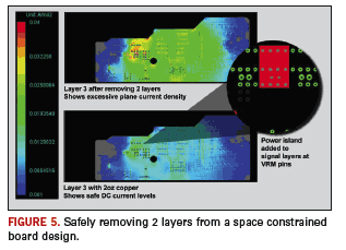
Comprehensive current density assessments can identify opportunities to safely reduce the plane layer count, leading to substantial cost savings. In one case, illustrated in FIGURE 5, a telecom equipment supplier hit the physical limit for board thickness. What-if DC simulations of current density for various configurations were used to confirm the potential to reduce layer count. Analysis of a design variation with two layers removed showed that most layers remained under defined current thresholds, with one layer showing excess current density. Design changes were considered to address the problem, and in the end, two changes improved the design. An additional ounce of copper was added to the layer that exceeded current density limits, and a power island was added to the design’s 10 signal layers at the VRM pin locations. Simulations of the new design confirmed that the three power plane layers could safely be reduced to one layer with maximum densities staying below the specified 20 mA/mil2 threshold. Beyond that, the resulting design was significantly less expensive to manufacture.

Design Flow Considerations
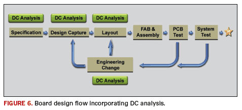
DC analysis throughout the design process enables design teams to predict and prevent problems to avoid costly late stage rework. The flow in FIGURE 6 has been demonstrated to improve design reliability and to prevent field failures. From a flow standpoint, communication between the DC simulation environment and the layout software used for the project is valuable. This can enable DRC style information to be seen while layout progresses to give cues for design improvement.

Simulations lead to design improvements that minimize the DC portion of the total AC / DC budget while assuring robust performance. A DC first approach is generally recommended with AC analysis quickly following to enable further adjustments for low-, mid- and high frequency noise.
In some flows, DC analysis results are exported as SPICE sub-circuits that can be used for further analysis for detailed thermal studies. For some designs, it is valuable to create compact DC-equivalent resistor models of multiple structures to facilitate system-level analysis, which can include PCB, IC package and on-chip models.
As noise margins compress, it is no longer practical to rely on spreadsheet approaches for DC assessment. When used for early planning and as layout progresses, DC simulation enables designers to manage risks and improve their designs. Selection of the best possible VRM and remote sense locations improves DC performance. IR drop and current density risks are often more difficult to identify than to resolve. The best DC analysis tools provide fast runtimes with the accuracy needed to isolate these obscure but significant threats.
Actionable feedback in the form of color mapped visualization and pass / fail checks builds a clear connection between the DC simulation and high-impact design improvements. Accurately simulating DC behavior to predict and prevent issues is far superior to waiting to find and fix problems late in the game. Left unresolved, excess current density and IR drop lead to product instability and field failure. Focus on a quality DC implementation avoids these problems and provides additional cushion to deal with AC noise. Further, an understanding of robust DC performance provides insight into overall AC / DC power delivery system behavior. DC simulation can be added to design flows without disrupting existing methodologies. The combination of easy implementation and the clear ability to improve every design make effective DC simulation an essential part of the PCB and IC package design process. PCD&F
References
1. International Technology Roadmap for Semiconductors (ITRS), 2007 Edition, System Drivers.
2. Sam Chitwood, Sigrity, Inc., “IR Drop in High-Speed IC Packages and PCBs,” Printed Circuit Design and Manufacture, April 2005, Pgs. 16-18.
LESLIE LANDERS is vice president of marketing at Sigrity, Inc; This email address is being protected from spambots. You need JavaScript enabled to view it. and TANIT VIRUTCHAPUNT is a power integrity specialist at Sigrity, Inc; This email address is being protected from spambots. You need JavaScript enabled to view it.


