Understanding material properties reduces the design cycle, facilitates stack up and provides a cost to performance advantage.
System operating speeds continue to increase to answer consumer demand for such technologies as faster Internet connectivity, video on demand and mobile communications. As a result, high performance printed circuit board (PCB) substrates have emerged to address signal integrity issues at higher operating frequencies, commonly called low Dk and/or low loss Df materials.
The published “typical” values found on a product data sheet provide limited information, usually a single construction and resin content, and are derived from a wide range of test methods and test sample configurations. A PCB designer or front end application engineer must be aware that making a design decision based on the limited information found on a product data sheet can lead to errors which can delay a product launch or increase the assembled PCB cost. To help designers, the following presents critical selection factors that go beyond a typical product data sheet and explains how these factors must be considered when selecting materials for high-speed applications.
Whether making a decision to buy electronic equipment, a mobile phone or substrate material, one of the first places a person looks is to the technical data sheet. The data sheet provides a snap shot of the product attributes that can be used to compare similar products. A laminate material data sheet should be used as a guideline and a comparison tool, not a design tool. It is, however, often used for that purpose.
The terms permittivity (Dk) and loss tangent (Df) are used on the data sheet to describe laminate electrical performance properties. Both of these properties vary with changes of resin content, temperature and moisture content of the substrate material.1,2 In addition to these factors, the test methods that are used to evaluate the laminate properties can produce values that vary significantly. A standard high Tg laminate data sheet states the “typical” electrical properties (Dk and Df), at 1 MHz to 1 GHz for one resin content. For high-speed digital substrates, a data sheet will provide “typical” (not exact frequencies) data points for 2 GHz, 5 GHz and 10 GHz for one resin content. In some cases, the data sheet will specify the test method that was used to test the material. A PCB designer will need more information about the test methods used to prepare the laminate electrical data in order to make informed decisions about which laminate is the right choice for the application.
Making an informed decision means the designer should consider the variations in the material properties as well as the test methods used to develop the material data, yet the typical data sheet does not provide this type of detailed information. As design requirements for high-speed digital applications continue to push the envelope of performance, it becomes critical to consider these influences.
Basis for Comparison
In order to understand the influence of material and test variations on electrical performance, one can use the following equations to approximate the dielectric and conductor losses that will be used as the foundation for comparisons in this article. It is important to include the conductor losses as part of the comparison, because that portion of the loss can account for a substantial portion of the overall loss. The calculation for conductor loss does not include the effects of surface roughness of the conductor and should not be ignored. Conductor loss as a result of surface roughness is outside the scope of this article.
The following first-order approximations can be used to show the difference in attenuation.8
EQ 1:
αmaterial = αdielectric + αconductor
αdielectric = 2.3 •ƒ • Df • √Dk (dB/in) where,
αdielectric is the dielectric loss
ƒ is the frequency (GHz)
Df is the material loss tangent
Dk is the material relative permittivity
and,
EQ 2:
αconductor = 36 • √(ƒ) / Zo • w (dB/in), where
αconductor is the conductor loss
ƒ is the frequency (GHz)
Zo is the impedance (Ω)
w is the trace width (mil)
These approximations have been demonstrated to be accurate enough to make informed decisions regarding material performance. These two equations will be used below to help demonstrate the influence of the variables mentioned previously.
Effects of Resin Content
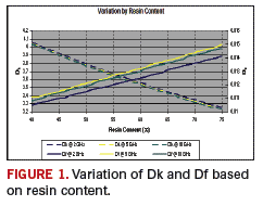
Differences in resin content percentages have a significant effect on the Dk and Df values. The resin content percentage varies based on the glass style, the target thickness for a given glass style and the manufacturing tolerances. FIGURE 1 demonstrates these differences between resins contents of 40% to 75% at three nominal frequencies at room temperature. Typical resin content percentages for laminate and prepreg product lines range from approximately 40% to 50% on thick cores with heavy glass cloth like 2116, 1652 and 7628 and 65% to 75% for 106 and 1080, which are typically used to bond innerlayer cores together. Typical thin core constructions in the 0.003 inch to 0.005 inch thickness range are around 50% for single-ply glass cores and in the 60% resin content range for two-ply glass cloth cores.

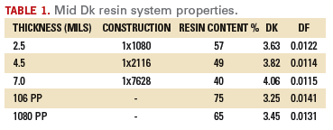
Different laminate thicknesses require different glass styles, and subsequently, different resin contents to achieve the desired thickness. Using a mid-Dk material operating at 2 GHz, from the example above, one can determine the values for the electrical properties for a single ply of 1080, 2116 and 7628 laminate and 106 and 1080 prepreg. Table 1 reveals how these values change with resin content.

Effects of Temperature
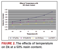
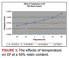
The reported values on the laminate data sheet are typically derived from testing at room temperature; however, the electrical performance of the substrate will also vary with the operating temperature of the PCB. Most high-end designs typically incorporate components that develop a significant amount of localized heat during operation. The designer should be aware of the influence of the material’s increased temperatures due to localized heat generated by the components mounted on the board. Selection of a material with a minimal response to increased temperatures should be considered when operating temperatures are elevated.
FIGURES 2 and 3 demonstrate that using a lower Dk and Df product provides a more stable performance over a wider range of temperatures. As an example, for a Mid Dk resin system between 23°C to 50°C, the difference in permittivity, Dk and loss tangent, Df is about 0.5% and 10% respectively. The change in permittivity is small while the difference in loss tangent is significant. The approximate increase in attenuation using EQUATION 1 is ~10% or -0.266 dB/in., versus -0.295 dB/in.


Effects of Moisture
As designers continue to push the design envelop and operating frequencies continue to increase, humidity dependant loss should be considered.2 The rate of diffusivity and the equilibrium moisture content can be calculated using Ficks’ Law of Diffusion for a given laminate using a specific resin system and thickness. Laminate data can be used for comparison between material choices and to make predictions about the potential influence during system operation. Moisture dependant electrical performance data is very difficult to define on a data sheet, but it should be considered.
The rate of moisture uptake of the material is dependent on several factors which include: ambient environmental and process temperatures, time of material exposure during fabrication, influence of wet PCB manufacturing processes, prepreg, etched laminate, PCB storage conditions, inner layer and PCB thickness, PCB packaging, resin type and resin content, PCB design and construction, all of which allow, introduce or trap moisture in the PCB. These factors influence the amount of moisture that might be in a PCB. The definition of each point of ingress cannot be easily modeled and is not easily predicted.
Effects of Differences in Construction
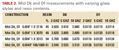
Laminate properties are dependent on construction because each construction is made using different glass styles and resin contents. The designer should be aware of the differences in Dk and Df values between single-ply and two-ply laminate constructions for the same thickness. A typical data sheet lists only one construction and one resin content and does not show the range of construction options. TABLE 2 compares single-ply construction to a two-ply construction showing that the electrical properties are significantly different within a given thickness. These differences do become critical when bandwidth is at a premium.

On an existing design, substituting a single-ply core for a two-ply core construction to save cost will result in differences in the laminate electrical properties. One common mistake that is made is a substitution of a single-ply laminate or prepreg for two-ply dielectric openings to save money and to offer a reduced cost PCB without consideration of the changes in electrical performance. The result may be a nonfunctional or poorly functioning system.
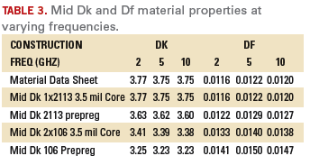
Compare the properties of laminate used in a design built using a 2 x 10⁶, 3.5 mil core and one substituting a single-ply 1 x 2113, 3.5 mil core. TABLE 3 compares the data sheet and the construction options for Mid Dk material. Given this information, one should note that the 1 x 2113, 3.5 mil core electrical properties are a relatively close match in the material data sheet, while the 106 and 2113 prepreg and 2 x 10⁶, 3.5 mil core are significantly different. This is a critical difference that must be considered when bandwidth budgets are tight.

Referring to Table 3, consider a PCB which has a 10-inch long, controlled impedance transmission line operating at 2 GHz that has been designed, tested and prototyped using the 2 x 10⁶ construction and correct dielectric properties. In an effort to reduce cost, the PCB shop might decide to convert the design to a single-ply stack up and substitute a 2113 construction for the 2 x 10⁶ dielectric openings. The problem arises when the line widths must be reduced to match the desired impedance due to the higher Dk values of the 1 x 2113 core and 2113 prepreg (which in this case matches the data sheet). In order to match impedance, the PCB engineer would typically calculate the line width based on a 50 Ω impedance target and would arrive at ~3.6 mils on half ounce copper. However, for the 2 x 10⁶ construction, the line width would be ~4.4 mils on half ounce copper.
By reducing the line width, the conductor losses increase, and this is where the substitution becomes a problem. The resulting attenuation, due to conductor losses alone, as determined by EQUATION 2 would be approximately -0.280 dB/in and -0.233 dB/in respectively. Combining these with the dielectric losses, the 2 x 10⁶ construction would result in an attenuation of approximately -3.44 dB, and the 1 x 2113 construction would result in an attenuation of approximately -3.83 dB. This is a 10% increase from the original construction and may result in system performance issues.
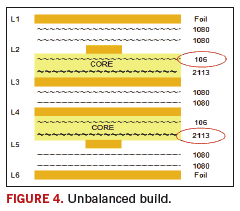
In another example shown in FIGURE 4, an unbalanced laminate construction also poses a potential risk. The local εr (Dk) on one side of the laminate in a 106/2113, 5.3 mil core construction will be different from side to side.6 Orientation of the panel during design and fabrication becomes critical and care must be taken to ensure the panel is printed on the correct side. The difference in the Dk and Df values from the 2113 to the 106 side is approximately 12% and 19% respectively.

The resulting difference in attenuation between the bulk properties and the local properties of a strip line configuration placed on the 106 side of the laminate using the construction above at 5 GHz, as determined by equation 1 would be -0.36 dB/in which would have a significant impact on the band width budget.
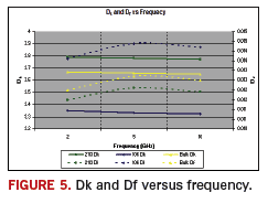
FIGURES 5 demonstrates the variation in the local dielectric properties as compared to the bulk properties. Note that the laminate test methods used to determine the bulk dielectric properties of materials cannot be used to take into account the localized effects of construction.

Differences in Resin Systems
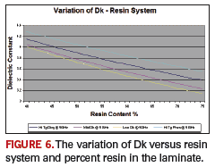
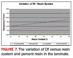
PCB designers and engineers must be careful to note that each resin system will have different Dk and Df values depending on resin content. A common mistake is making a substitution from one resin system to another without fully understanding the differences in material performance. This often results in boards that do not function at all. One example of this error is the substitution of a High Tg lead-free Phenolic-cured resin system versus a High Tg non lead-free Dicy cured resin system. This error can occur when the electrical properties are not fully investigated and the performance of the Phenolic-cured system falls short. FIGURES 6 and 7 demonstrate the differences between four resin systems.


TABLE 4 compares the four materials at 50% resin content. Note the significant difference in material performance between resin systems.

By using Equation 1 we can evaluate the difference and benefit of using lower Dk/Df laminate materials. A simple estimated bandwidth analysis at 5 GHz gives the following results: -0.527 dB/in, -0.395 dB/in, -0.271 dB/in and -0146 dB/in respectively. In theory, the line length could be 3.6 times longer depending on the dielectric material used.
Differences in Test Methods
The methods commonly used for testing laminates are Parallel Plate, Two Fluid Cell, Split Post Cavity Resonator, IPC X-Band Stripline, Bereskin Stripline and Full Sheet Resonance methods. All of these methods have limitations that are dependant on the sample thickness, frequency used for the test, accuracy of the test method and repeatability of the measurements.3,4,5 Because of the number of different test methods and resin contents used by laminate suppliers, it is extremely difficult to make an accurate comparison between laminates using the data sheet.
The applicable test frequency range, sample requirements and accuracy of the results vary depending on the method used. The test fixture also plays a role since air gaps between the samples and the fixture can skew the results. And indeed, the differences in fixtures for the same method produce significant differences in test values due to air gaps.
The first two methods listed in TABLE 5 are commonly used for standard epoxy laminates, but they are not capable of providing adequate information for HSD (High-Speed Digital) designs above 2 GHZ. The IPC Stripline Method is well suited for HSD but has a limited range of test frequencies. The Bereskin Stripline Method has the advantages of the IPC Stripline test method but offers a wider range of test frequencies.

The Bereskin Stripline method has been demonstrated to correlate well with both FEA techniques and actual PCB board testing.5 By employing equations 1 and 2 with the data collected using the Bereskin Stripline Method, one can determine the approximate attenuation and compare the results. This type of analysis is critical to understanding how the laminate data compares to simulator generated data and actual PCB measurements.
The Split Post Cavity method appears to offer a wider range of test frequencies and better tolerances; however, the values may not correlate as well with actual PCB board test data. In the IPC test method7 IPC-TM-650 2.5.5.5 Section 1.3 (Stripline Test), it is clearly stated “…users are cautioned against assuming the method yields permittivity and loss tangent values that directly correspond to applications. The value of the method is for assuring consistency of product …” It is clear that the only true way to understand the usefulness of laminate data produced by these methods for design purposes is to perform adequate correlation studies between the method(s), actual measured test vehicles and software analysis/simulations.
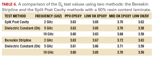
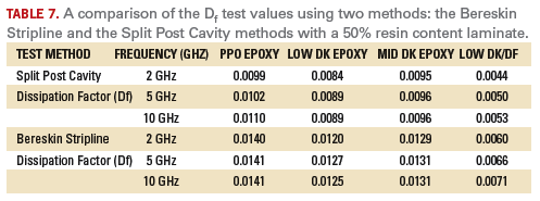
To further define how these methods produce significantly different data sets, TABLES 6 and 7 compare the Dk and Df test values using two methods: the Bereskin Stripline and the Split Post Cavity methods with a laminate resin content of 50%. The Dk testing yields only slightly higher values using the Bereskin Stripline method when compared to Split Post Cavity method. Therefore, for the purpose of Dk testing, the two methods are very comparable and yield similar results.


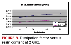
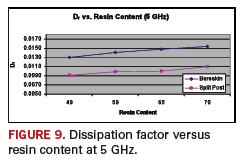
However, when testing identical samples using these two methods, the differences become apparent when comparing the Df values (FIGURES 8 and 9). The values for the Split Post Cavity Method are 20% to 30% lower for each material than for those derived using the Bereskin Stripline Method. When comparing laminate data sheets, the designer should be aware that the product tested using certain methods may appear to have better loss properties than a product tested using the another method.


A Problem with Substitution
A major problem can arise when material substitutions are made using laminate data sheets as a guide, especially when the data is derived from different laminate test methods. While initial impedance calculations look acceptable because the Dk values are similar, the actual board performance may be significantly different and may result in poorly functioning or non-functioning boards. Matching the Dk is important, but matching the Df is critical.
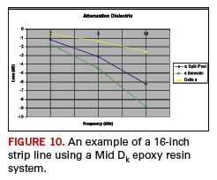
FIGURE 10 illustrates a 16-inch strip line using a Mid Dk epoxy resin system. Using Equation 1, with no conductor losses included, it can be determined that the difference between data derived from the Split Post Cavity Method and that derived by the Bereskin Stripline Method is as large as -2.54 dB at 10 GHz which is over 80% of the typical -3 dB budget for a typical transmission line.

Making a material substitution is a serious endeavor. A lack of understanding of the actual material properties can result in costly mistakes.
Conclusion
Data sheets do not provide adequate information for design purposes. The laminate supplier should provide detailed information about the laminate performance over a range of resin contents and frequencies. They should demonstrate expertise and complete understanding of the test method(s) used to acquire the data and how it relates to other methodologies, including PCB and system test methods. More complete information can assist in reducing the design cycle and prototyping steps and aid the designer in making stack up selections that reduce cost and/or provide a cost to performance advantage. Furthermore, characterization of the material in a standardized test vehicle should be performed to fully understand the performance of high-speed digital materials.
Data sheets can be useful tools during an initial material electrical properties comparison, if the test methods used to derive the data are identical. Care should be taken to fully understand any differences between the test methods used to derive the properties as they may produce significantly different results. Differences in the test method can make a one-to-one comparison misleading and can result in major performance issues when a laminate substitution is made and may potentially result in a nonfunctioning system. One of the most common mistakes that is made is making a material substitution without considering the actual electrical performance properties of the laminate material. PCD&F
Michael Gay is the director of emerging products for Isola Group. He can be reached at This email address is being protected from spambots. You need JavaScript enabled to view it.. Rich Pangier is the director of OEM marketing for the Isola Group. He can be reached at This email address is being protected from spambots. You need JavaScript enabled to view it.
REFERENCES
- Khan, Subhotosh PhD; “Comparison of the Dielectric Constant and Dissipation Factors of non-woven Aramid/FR4 and Glass/FR4 laminates,” Volume: 26 Issue 2, Circuit World, June 2000.
- P. Hamilton, G. Brist, B. Guy Jr and J. Schrader; “Humidity-Dependent Loss in PCB Substrates,” IPC/APEX Expo February 2007.
- Neves, Bob; “Permittivity/Dielectric Constant: Do the Math,” CircuiTree November 1996.
- F. Hickman, S. Bertling; “Dk/Df Testing Methods,” TPCA November 2004.
- S. Mirshafiei and D Enos, Signal Integrity Analysis Techniques Used to Characterize PCB Substrates,” IPC/APEX April 2004.
- G. Brist; “Design Optimization of Single-Ended and Differential Impedance PCB Transmission Lines,” Presentation p. 100.
IPC IPC-TM-650 Test Methods Manual
- Bogatin, E., “Lossy Transmission Lines; Plain and Simple,” Presented at PCB West, March 2002.


