Early design decisions can improve solder mask registration on fine-pitch products, resulting in significantly higher assembly yields.
The evolution of surface mount technology (SMT) is toward the use of smaller and higher I/O components for new electronics applications, including portable and hand-held products. This drives a need to reduce size and increase interconnect density for new area array packages. The assembly process for ball-grid array (BGA) and chip-scale packages (CSP) has stabilized over the years.1 However, products using fine-pitch BGA/CSP components at 0.8-mm pitch or below still pose many assembly challenges, including solder short prevention and detection.
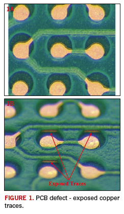
When implementing fine-pitch BGA/CSP components into production, experience has shown that some assembly process issues can be caused by solder mask misregistration that occurs during printed circuit board (PCB) fabrication. Misregistration of solder mask can commonly approach +/- 0.003 inches from the datum point; however, this typically does not create problems in standard SMT processes. As the industry continues to use more array components with ball pitches of 0.8 mm and less, the opportunity for defects associated with solder shorts that are related to solder mask design and registration becomes more prevalent. Solder mask misregistration can cause issues with exposed adjacent traces and/or vias underneath array packages, thus increasing the opportunity for shorts. FIGURE 1 shows an example of an exposed trace due to solder mask misregistration. Note that the exposed copper traces are not visible from the top view (FIGURE 1A), but are visible when viewed from an angle (FIGURE 1B).

Consequently, the solder mask coating process quality is a critical concern for high-density boards containing fine-pitch BGA/CSP devices and has an impact on the assembly process. The acceptable solder mask registration criteria must be more stringent than standard PCB solder mask fabrication requirements. Therefore, proactive design and fabrication considerations should be followed to improve assembly yields.
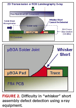
When a trace is exposed due to solder mask misregistration, solder bridging may form during the solder paste screen-printing process. Misalignment of the solder paste printing process could aggravate the bridging issue. Placement of the fine-pitch component would further spread the solder paste into the solder mask cavity. During reflow, the hot-slump phenomenon spreads the molten solder and causes solder bridging. When the solder joint solidifies after reflow, a minute solder bridge would be formed between the pad and the exposed trace or via. Typically, this minute solder bridging of pad to the exposed adjacent conductor or via is very small (about 1 mil to 2 mils thick) and is referred to as a “whisker” short. FIGURE 2 shows a cross-section view of a solder joint with whisker short and with x-ray examinations. The whisker short could not be detected using 2D transmission x-ray because the image density of the solder ball diameter would overshadow the whisker short. Similarly, laminography x-ray (5DX) could not reveal the whisker short. Therefore, whisker shorts to adjacent traces or vias are very difficult to detect following fine-pitch BGA/CSP assembly; the only solution would be to remove the components and inspect the fine-pitch BGA/CSP site. This solder short defect may require many hours to diagnose, and was observed only after the fine-pitch BGA had been removed.

To resolve solder mask misregistration concerns during PCB fabrication, companies must create specifications in the fabrication notes to explicitly indicate unique solder mask registration requirements. Also, critical areas such as fine-pitch BGA/CSP sites must be identified to the PCB fabrication vendors and assembly providers requesting a thorough inspection of those areas. The IPC-A-600 specification2 can be used as a supplement to a company’s specifications. Additionally, this solder mask misregistration feature can be used as a quick diagnostic if an assembly has an electrical short at the fine-pitch BGA/CSP component location that is not detected by x-ray processes.
Solder Mask Registration Control
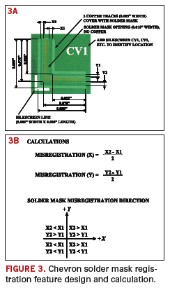
A special solder mask registration feature called a “chevron”, as shown in FIGURE 3A, has since been implemented on designs with 0.8-mm or smaller pitch area array devices to assist with solder mask registration verification. This registration feature consists of two 0.005-inch copper traces and a 0.010-inch solder mask opening slot. The solder mask slot is placed between the copper traces, and all three features are laid out in an “L” shape. A 0.005-inch space is designed between the solder mask slot and each copper trace. The recommended overall dimension for chevron design is 0.080 square inches. However, the dimensions can be adjusted to any reasonable size as long as the “L” feature is observable and the spacing is equal to or greater than 0.005 inches between the copper trace and solder mask slot. This allows for standard copper etch or solder mask process variations such that measurements can still be made if the copper trace or solder mask opening is over or under etched. An additional silkscreen trace is added along the outside corner of the “L” shape to evaluate the silkscreen dimension and registration. This silkscreen is 0.005 inches in width and 0.020 inches in total length.

As the solder mask shifts relative to the copper artwork, a measurable offset can be identified in both X and Y directions by taking the difference between the measurements and dividing by two (FIGURE 3B). The positive or negative sign of the calculation indicates the direction of solder mask misregistration. For example, if X2 > X1, then the solder mask has shifted toward the positive X direction of the Cartesian coordinate system. The same principle applies for Y. If Y2 >Y1, then the solder mask has shifted toward the positive Y direction.
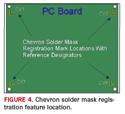
To verify solder mask registration, a minimum of three “chevron” solder mask registration features are recommended at the corners of the PCB to assist in solder mask registration verification (FIGURE 4). If the solder mask registration features are located on break-off tabs of a PCB panel, the break-off tabs could be removed prior to the test process, and the solder mask registration features would not be available for failure analysis. In this case, the solder mask misregistration issue cannot be identified unless the fine-pitch BGA/CSP component is removed from the PCB. Therefore, the preference would be to have the solder mask registration features on each PCB module. The solder mask registration features could be located close to the global fiducials while observing fiducial clearance requirements. It is also helpful to have a component reference designator, such as CV1, next to each solder mask registration feature for inspection and measurement reference.

To further reduce the possibility of a solder mask registration problem, the customer’s initial PCB design needs to be reviewed for design for manufacturing (DFM) violations. The updated design should then be reviewed with a PCB supplier to minimize solder mask misregistration issues. It is also important to note that different PCB vendors will use different solder mask openings, so they must be alerted to the special requirements for fine-pitch BGA/CSP2,3. Minimizing solder mask clearances around array pads can reduce this problem; however, it also may reduce the number of capable vendors.
Vendors should also include a capability study (Cpk) on solder mask registration and have a history of producing fine-feature PCBs. Vendors should be able to perform up-front DfM review of the PCB layer design and provide details on solder mask opening and alignment tolerances for critical fine-pitch BGA/CSP applications. The vendors should use an electronic DfM tool that provides design rule checks (DRC), and the DRC should be reviewed by customers and PCB vendors prior to the start of board fabrication.
From the perspective of the assembly provider, receiving inspection must be equipped with adequate microscope measurement capability for inspection of fine-pitch BGA/CSP or high-density areas. The recommended magnification is 10X minimum for 0.8-mm pitch, 15X minimum for 0.65-mm pitch and 20X minimum for 0.5-mm pitch components. A heightened sampling plan should also be established to obtain measurements of the chevron registration marks and should be performed on a predetermined basis.
Conclusion
Solder shorts under fine-pitch BGA/CSP components caused by solder mask misregistration can be very difficult to detect on a completed PCB assembly using a standard x-ray processes. To better control solder mask design and registration, a set of chevron solder mask registration features can be designed on the board to aid vendors and assembly providers in obtaining verification of solder mask registration during inspection. If a defective PCB assembly is suspected of solder shorts under the fine-pitch BGA/CSP component and has not been detected by x-ray, the solder mask registration features can be used as a debugging tool without having to remove the fine-pitch BGA/CSP component. This will ultimately reduce time and cost for investigation of the solder short defect.
With additional considerations to reduce the possibility of a solder mask registration issue, PCB vendors’ capabilities on solder mask registration tolerance should be well understood, and the solder mask registration tolerance and requirements should be included in the design fabrication drawing. For the assembly provider, critical areas, such as fine-pitch BGA/CSP sites, should be identified and conveyed to receiving inspection personnel. The inspection criteria may require sampling of the fine features with proper equipment, such as microscopes with measurement systems and adequate magnification.
With the registration monitoring feature design and proper board fabrication considerations, solder mask registration issues can be minimized and possibly eliminated. The time invested on the PCB design review and verification of solder mask registration will result in better assembly process and higher yields. PCD&F
Acknowledgements
The author would like to thank Tom Cipielewski, Paul Neathway, Quyen Chu and Peter Verbiest of Jabil’s Global Operations Services Manufacturing Engineering for their contributions and supports.
References
- Ken Gilleo, Area Array Packaging Handbook, New York, McGraw-Hill, 2002, pp. 18.4-18.11.
- IPC Committee, IPC-A-600F Acceptability of Printed Boards, Illinois, IPC, 1999, Section 2.9.1 - 2.9.3.
- IPC Committee, IPC-7095 Design and Assembly Process Implementation for BGAs, Illinois, IPC, 2000.
Hien Ly is a senior manufacturing engineer at Jabil Circuit, Inc. and can be reached at This email address is being protected from spambots. You need JavaScript enabled to view it..


