Fine-pitch BGAs dramatically increase in pin count and will drive adoption of HDI.
The previous articles have focused primarily on fanout and routing of large (over 1500 pins) BGAs with a pin-pitch of 0.8 mm or 1.0 mm. However, many of the queries I get from designers pertain to devices with a pitch less than 0.8 mm. Most of these queries are about 0.6-mm pitch, but some of them are about 0.5-mm and even 0.4-mm pitches. These devices are used commonly in handset products such as cell phones and PDAs. Just this week, I met a designer who completed a credit-card sized board that had seven BGAs on it!
Most smaller BGAs have relatively few pins – generally fewer than 200. The primary problem designing with these BGAs is to route out of the array requires very small features, making the design difficult to fabricate at a low cost and with high yields. But just when you thought that fine-pitch BGAs would remain with a small pin-count, get ready for some new processors with 600 pins on a 0.6-mm pitch.
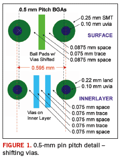
Unfortunately, with the small devices, there is not much that can be done with fanouts to improve the route density. Nevertheless, this “not much” may be sufficient to help with your particular design. At this scale, there is only room to put a via-in-pad, so we need to look at methods for via placement that will enable additional traces in the route channels between the vias on the inner layers.
As a general note, the design rules for these very fine pin-pitch devices will have to be smaller than what is used with a standard FR-4 board. By using HDI, the traces can measure 0.75 mm and the micro-via pad can measure 0.25 mm with a 0.10-mm hole.
Shifting Via-In-Pad
FIGURE 1 illustrates the positive impact of shifting the via inside the pad just slightly to increase the center-to-center spacing to 0.595 mm. This will enable two traces between the vias, resulting in every other channel having two traces.

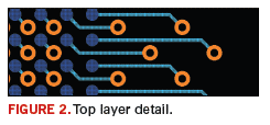
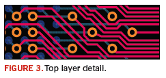
Another method, that applies to BGAs of all sizes, is to spread the perimeter vias away from the device that allows additional rows of ball pads to be escaped on fewer layers. I described it in the context of 0.8-mm devices, but it also can be used for 0.6 mm and below. This technique allows for an extra two rows of I/Os to be routed on the first signal layer. In most cases, this will result in a reduction of one signal layer for escaping the BGA. One signal layer may not sound like much, but depending on your situation, it may actually mean you can reduce the stackup by two signal layers because the symmetry of the stackup require two layers to be added together.
FIGURES 2 and 3 illustrate this technique of pushing the fanouts out and away from the perimeter. The intent was to move the vias far enough out so that three traces could be routed between them on the diagonal. In the center of the BGA, I used a simple matrix dog-bone pattern that opens up the route channels in the center rows and columns; however, the method is also valid when putting the vias in the center of the ball pad or when shifting them.


I met with one designer who applied this technique on a number of fine-pitch BGAs and found that the additional area needed resulted in a total area similar to the 1-mm pitch. He then questioned the value of using such small BGAs. The miniaturization of ICs that enables increased functionality and performance at a lower cost often pushes new difficulties onto the PCB designer’s desktop. We can’t stop the progress of technology, but we can be thankful that our industry continually challenges us to develop new design methods.
Conclusion
BGAs with a pitch at 0.6 mm or less will become more common over the coming years, and the number of pins will increase dramatically. The impact on PCB design is significant and will drive adoption of HDI; however, you can eliminate one to two layers with the above techniques. pcd&f
Charles Pfeil is an engineering director for Mentor Graphics, Systems Design Division. Email: This email address is being protected from spambots. You need JavaScript enabled to view it..


