The glass weave in a laminate can affect propagation velocity and loss profile, leading to signal loss and skew in differential pairs.
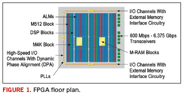
As data rates continue to increase, PCB designers are moving toward serial buses with differential signaling. High-speed serial interfaces such as PCI-Express, 10 Gigabit Ethernet XAUI, OC768 and CEI use differential signaling for transmitting and receiving data. FGPA devices with embedded high-speed transceiver blocks provide an easy, cost-effective approach for implementing these high-speed applications, as illustrated in FIGURE 1.

Differential signaling uses two output drivers to drive two independent transmission lines. One driver carries one bit, the other its complement. The difference of the two signals, measured between the two traces, carries the desired information. A differential pair is a pair of transmission lines with some amount of coupling between the two legs of the pair.
Ideally, routing a differential pair on a PCB should meet two criteria. Electrically, the two traces should be identical. This means each trace of the differential pair should have the same cross sectional dimensions and must be surrounded by the same type or types of dielectric materials. The spacing between the two traces should also be the same for the entire length of the trace.
Skew or time delay between the two traces of the differential pair should be zero. Thus, the edge of the difference signal is sharp and well defined. Any skew between the two traces results in a common mode noise and also leads to a degradation of the differential signal.
Dielectric Material Selection
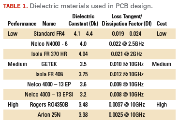
Proper dielectric material selection enables the PCB designer to minimize the dielectric loss because at frequencies above 1 GHz, dielectric loss is dominant compared to conductor loss. The dielectric loss is dependent on the loss tangent/dissipation factor for a given dielectric material. The lower the loss tangent, the better it behaves at higher frequencies and from a signal loss standpoint. The dielectric constant and the loss tangent information for the various dielectric materials typically used in the PCB design are shown in TABLE 1.

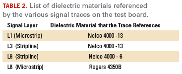
A test board with different dielectric materials and glass weaves was specifically designed to study the various aspects of the high-speed channel design. The test board was designed as an 8-layer board with four routing layers (L1, L3, L6, L8) and referencing different dielectric materials. Layers L2, L4, L5 and L7 are solid metal planes stitched together with through hole vias. They act as the return path for all the signal layers. The test board is a single-sided board with all the SMA (subminiature version A) connectors located on the top layer (TABLE 2).

The board uses three materials, Nelco 4000-13EP, Nelco 4000-6 and Rogers 4350B, allowing comparisons among different dielectric materials. All the test structures on the board were routed to meet a 50 Ω ± 10% single-ended impedance or a 100 Ω ± 10% for differential impedance. Wide trace widths are used to minimize conductor losses. Two identical differential pairs measuring 25 inches and 40 inches are routed on L1, L3, L6 and L8 to test the performance of various dielectric materials. Differential via design is optimized with ground return vias added next to signal vias to make the vias transparent1. The signal vias on L3 and L6 are back drilled to minimize via stubs.
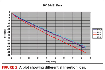
Vector network analyzer (VNA) and eye diagram measurements are used to study the performance of the various dielectric materials in frequency and time domain. Figure 2 shows a plot of the differential insertion loss for the 40-inch trace through 8.5 GHz. The measurements are limited to 8.5 GHz due to equipment limitations. Differential insertion loss results indicate the trace on L8 has the best performance because Rogers 4350B has the lowest dissipation factor. The microstrip and stripline traces on L1 and L3 have the next-best performance (Nelco 4000-13), followed by the trace on L6, which references Nelco 4000 - 6 dielectric material.
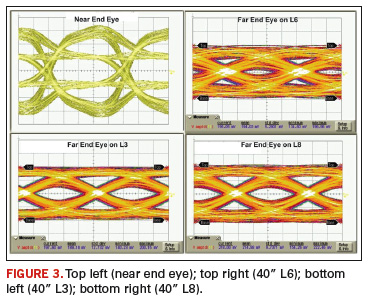
A similar insertion loss behavior, similar to the one illustrated in FIGURE 2, is observed for the 25 inch traces. In addition to the VNA measurements, eye diagram measurements are taken at 10 Gbps using a VOD of 600 mV with a pre-emphasis of 14.5 dB. Near-end and far-end eye diagrams before and after 40 inch traces on L3, L6 and L8 are shown in FIGURE 3. The vertical and the horizontal scale for the eye diagrams are 50 mV/division and 20 ps/division respectively.

For cost sensitive designs with lower interconnect lengths, the regular FR-4 type of substrates can still be used with a roughly ~2 dB performance hit compared to expensive substrates. PCB designers can use the built-in, pre-emphasis and equalizer settings in the transceivers available in Stratix GX series of FPGAs to compensate for a portion of the channel loss as the signal traverses through the backplane.
For current edge rates of tens of picoseconds (ps), PCB designers can gain an optimal price versus performance solution by moving from regular FR-4-based substrates to a mid-performance substrate such as Nelco 4000-13 EPSI, Isola FR-408 or GETEK material. The cost difference is relatively small in comparison to a high-performance type of material. The eye diagram observed on L8 references Rogers material (FIGURE 3) and shows the Vp-p magnitude of 218 mV compared to Vp-p magnitude of 198 mV on L3 and 195 mV on L6. In real applications, the true performance of Rogers material will be better than the observed eye on L8, provided there are no bandwidth limited components like SMA connectors on the board.

Fiber Weave Effect
The secondary impact that a dielectric material can have on a high-speed channel design is skew. A typical PCB dielectric (core/prepreg) substrate is constructed by combining woven fiberglass fabrics with epoxy resin. The woven fiberglass is needed to provide strength and structural integrity to a dielectric material.
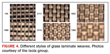
FIGURE 4 shows typical laminate weaves. The numbers next to each diagram identify the glass fabric style based on the fiberglass thickness, pitch, yarn and the number of glass fiber strands used. The glass and the epoxy each have different relative permittivity (Er/Dk) values, thereby presenting a non-homogenous medium for signal propagation.

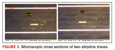
PCB designers usually route traces in multiples of 90° angles. A routed trace can land directly on top of the warp yarn (length), on top of the fill yarn (width), centered between the strands of warp yarn or centered between the strands of the fill yarn. FIGURE 5 is a microscopic cross section view of strip line traces landing on and off the weave.

Assuming that the two traces in Figure 5 comprise the two legs of the differential pair (P and N), they experience two different Er values. This in turn results in different propagation velocities and loss profiles. At high data rates, the difference in propagation velocities leads to skew between the two legs of the differential pair. Depending on the data rate, it can amount to a substantial fraction of the unit interval (UI). The skew between the P and N legs results in common mode noise and also leads to a degradation of the differential signal.
Substantial work has been done in the industry to study this effect2-5. To mitigate the skew associated with fiber weave, some of the techniques that are currently being used in the industry include the use of wider trace geometries to achieve impedance targets. The downside is that an increase in PCB area is needed to route all traces with wider geometries compared to narrow trace geometries.
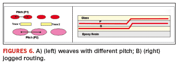
For strip line traces (FIGURE 6A), the PCB designers can use two different weaves with different pitches for top and bottom substrates to average out the effect. FIGURE 6B shows an example of offset traces. The intra-pair spacing forces each trace onto the path of its neighbor, regardless of glass pitch. Making use of a core or a pre-preg material with a denser weave, like 2116, 2113, 7268 or 1652, compared to a sparse weave, like 106 or 1080, during the PCB design process can reduce the fiber weave effect. For a marginal cost increase, PCB designers can use a substrate like Nelco 4000-13EP SI, where the difference in Er between glass and epoxy is smaller compared to a regular FR-4 based substrate.

Conclusion
PCB design takes on new dimensions involving high-speed applications with serial busses at multi-gigabit data rates. Designers must carefully evaluate the various dielectric materials and choose a material that is appropriate for the application since it directly impacts the signal loss and the skew seen on a PCB. PCD&F
References
1. AN529: Via Optimization Techniques for High Speed Channel Design. (www. Altera.com)
2. Scott McMorrow and Chris Head, “The Impact of PCB Laminate Weave on the Electrical Performance of Differential Signaling at Multi-Gigabit Data Rates.” DesignCon 2005.
3. Jeff Loyer, Richard Kunze and Xiaoning Ye, “Fiber Weave Effect: Practical Impact Analysis and Mitigation Strategies.” DesignCon 2007.
4. Gustavo Blando, Jason R. Miller and Istvan Novak, “Losses Induced by Asymmetry in Differential Transmission Lines.” DesignCon 2007.
5. AN528: PCB Dielectric Material Selection and Fiber Weave Effect on High Speed Channel Routing. (www.Altera.com)
Ravindra Gali is a senior design engineer with Altera Corporation and can be reached at This email address is being protected from spambots. You need JavaScript enabled to view it..


