System-level PCB emissions analysis reduces re-spins and EMC issues when PCBs are incorporated into larger systems.
For PCB and package designs, the issues of crosstalk, reflections, skew, ringing and other classical signal integrity challenges are pervasive and growing. A meaningful assessment of such effects requires system-level consideration to reliably account for coupling among traces as well as planes, vias and other design structures. System-level analysis also enables consideration of power integrity issues, such as power dissipation, thermal issues, current constraints and power plane noise. Distinctions between signal integrity (SI) and AC power integrity (PI) have blurred, and the need for design-side consideration of EMC has escalated. Simultaneous switching noise (SSN) is a perfect example of the coupling between SI effects and the underlying PI root cause. It is often the case, as for DDR memory circuits; this same SSN situation causes excessive power plane emissions and results in EMC issues. Therefore, system-level SI, PI and EMC are much more closely related than most designers realize.
Relationship Between SI and PI
Two of the first concepts electrical engineers learn are: current flows in loops and voltage is the potential difference between two points. These two simple concepts mandate the interdependency of SI and PI for printed circuit board (PCB) and package designs. To understand this concept, consider a signal net in a typical PCB design. Current flows in the signal net from driver to receiver, and so-called “return” current flows in the power/ground planes back to the driver to complete the required loop. There is a transient voltage at any point along the signal net. However, this voltage is not uniquely defined in the absence of a second point, often called a “reference” point. The voltage of interest at the driver is between the output pin and a local power/ground pin. Similarly, the voltage of interest at the receiver is between the input pin and a local power/ground pin. As these two voltages reference different local points in the power delivery system (PDS), any variation across the PDS is seen as a variation in these voltages.
There are many sources of variation in a PDS between the driver and the receiver reference pins. One example would be system-level effects. A DC voltage drop will exist due to the finite conductivity of the copper. Time delay for return currents becomes significant as rise time decreases, and power plane resonances can exist. All of these system-level PI effects are directly reflected in the driver and the receiver transient voltages. Localized effects include return path discontinuities, of which power plane splits and multi-layer via transitions are the most common. These discontinuities disrupt flow of the signal (SI effect) and also serve to locally couple energy from the signal into the planes of the global PDS. In fact, they are often a dominant source of power plane noise. In driver and receiver transient voltages, these system-level and localized PI effects are indistinguishable from more classical SI effects. SI and PI are not only related, but also inseparable.
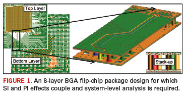
FIGURE 1 shows an 8-layer, BGA flip-chip package design for which SI and PI effects are tightly coupled. Ground nets are dark green, power nets are copper and signal nets are other colors. These two differential pair signal nets are modeled at first with circuit analysis. A frequency-dependent W-element model is applied for the differential pairs on the top layer and augmented by a parasitic inductance and capacitance to model the via transitions and ball grid array (BGA) pads. To verify the fidelity of this relatively quick and easy circuit model, a 3D EM analysis is performed. Computational capacity limits imply that the analysis only can be performed on the portion of the package shown in FIGURE 1. The circuit analysis and 3D EM analysis results are nearly identical, and most designers would comfortably consider the design completed. However, performing a system-level analysis of the whole package, including all coupled SI and PI effects, demonstrates a power plane resonance that significantly perturbs the transmitted, reflected and coupled signals on these two differential pairs within the frequency band of interest.

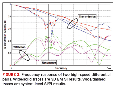
FIGURE 2 shows S-parameter results for this design. The 3D EM results are shown as solid traces and the system-level results as dashed traces. Two sets of traces with similar but divergent behavior are seen for each type of analysis that results from length differences between the differential pairs. At about 40% of the maximum frequency, the transmitted signal decreases signficantly and the reflection is nearly as large as the transmission. At this frequency, a resonance on the power planes occurs. This global PI issue dramatically affects the perceived SI behavior of the design. Without system-level analysis, this design would have proceeded to manufacturing release and resulted in performance failure for the packaged device.
SI and PI Analysis Tradeoffs

Circuit analysis SI results are very quick and easy to obtain for this design. Transmission line calculators can determine the time delay and the impedance of the differential pairs on the top layers, and via parasitics can be estimated based on previous experience or approximate equations. This circuit model yields enough accuracy for higher-order circuit analyses, such as reflection or timing budgets. Circuit analysis implicitly references all voltages to global node 0, which implies a “global ground” and precludes the consideration of all PI effects. The fidelity of the circuit model could be improved by using 3D EM analysis results for the via transitions.
3D EM analysis of an entire design can yield highly accurate results and is ideal for detailed component design such as crafting a via padstack and return via locations for a high-speed channel. However, significant computational resources are required, and only a small portion of complex PCB or package designs can be considered in a single analysis. In the previous example, the power planes were truncated a reasonable distance from the signal nets of interest – sufficiently far to capture local PI effects of return path discontinuity but not to capture global PI effects (a resonance in this case). Complex designs usually lack the computational capacity for 3D EM analysis to adequately consider PI issues.
Not surprisingly, the circuit and 3D EM analysis results were similar. The via transitions and return paths were carefully crafted to avoid localized return path discontinuities. Local to the differential pairs, the circuit analysis assumption of an ideal global ground return path was very close to the structure of the design.
The system-level analysis applied is a hybrid combination of circuit analysis and EM analysis. Circuit-level analysis is applied to concatenate the models of all components, such as: traces, vias, pads and wirebonds. 2D and 3D EM computations are applied to obtain electrical models for each circuit component; 3D EM analysis handles power planes. The circuit and the 3D EM analyses are merged into one fully coupled hybrid analysis. All local and global, SI and PI effects are considered by such hybrid analysis. This analysis predicted the plane resonance effect of the complex package design, which circuit analysis precluded and 3D EM analysis did not have the capacity to include in the physical model. However, this type of system-level analysis is more complex than circuit analysis and, therefore, more computational-intensive. Unlike 3D EM analysis, circuit analysis techniques are leveraged only in part, but the advantages include greater capacity and faster analysis of orders-of-magnitude. The package design required only minutes of setup time and seconds to perform circuit analysis, versus 30 minutes of setup time and more than a day of computation time for 3D EM analysis of a portion of the design, not to mention 15 minutes of setup and a few hours of computation time for hybrid analysis of the entire package.
Simultaneous Switching Noise: A Combined SI and PI Challenge
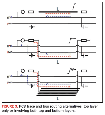
SSN challenges are a paragon of inseparable signal effects and power plane behavior. SSN effects exist even if all signal-to-signal coupling is ignored. However, when power plane (return path) effects are ignored, SSN no longer exists. To explore SSN, a simple 4-layer board was defined – a signal layer on top and bottom with one power and one ground plane layer in the middle. As a reference design, a signal net was routed from drivers to receivers on the top layer only. The same signal net was then routed with a significant portion of its length on the bottom layer of the board. This multi-layer routed net was duplicated to form a parallel bus to investigate SSN. These three designs are shown schematically in FIGURE 3. To transition from top layer to bottom layer, the via transitions must pass through both the ground plane and power plane, causing a discontinuity of return path – a PI issue. To enable this return path change from one plane to the other, the planes are connected through decoupling capacitors placed locally to the via transitions.

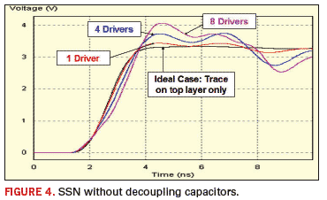
FIGURE 4 shows the transient voltage at the receiver load of these three designs characterized with system-level hybrid analysis. The black trace is the ideal case of routing a single net only on the top layer. The red trace corresponds to routing a single net on both top and bottom layers with multi-layer via transitions. Only slight rise time degradation (skew) is observed in single-layer routing, with a low level of signal ringing. In multi-layer routing for a bus structure of four or eight nets, the SSN condition of all drivers switching at the same time demonstrates increased skew and increased ringing as the bus width increases.

Net lengths were intentionally kept short to avoid proximity coupling effects. The results are unchanged for circuit analysis if this circuit-level effect is intentionally ignored in the hybrid analysis. Circuit analysis ignores PI effects and, for all cases, predicts exactly the same rise time degradation and maximum overshoot as for the ideal single-net, single-layer case.
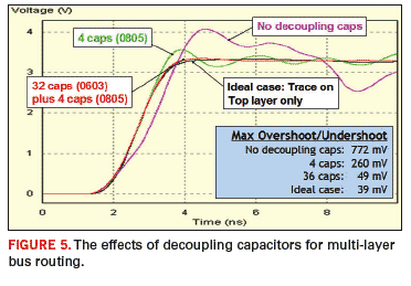
FIGURE 5 shows the transient voltage at the receiver load of SSN condition for the multi-layer bus with eight drivers. The black reference trace for single-net, single-layer routing and the violet trace for the bus are duplicated from Figure 4. The addition of four, large-valued, 0805 capacitors yields the yellow curve. The skew is eliminated and the maximum overshoot is reduced from a completely unacceptable level of 772 mV to a better, but still troublesome, 260 mV. The addition of two, smaller-valued, 0603 decoupling capacitors local to the two via transition regions yields the red trace. Maximum overshoot is dramatically reduced to 49 mV, just 10 mV higher than the ideal case of single-net, single-layer routing.

The implicit global ground applied precludes PI effects; therefore, decoupling capacitors are not included in circuit analysis. A semi-numerical and approximate analysis technique can be implemented to apply circuit analysis techniques by gridding power/ground planes and representing local RLC parasitics for each grid point. However, this approximate PI analysis cannot include signal nets. 3D EM analysis of this simple example could be performed without reaching computational capacity limits. Though nearly identical analysis results are achieved by 3D EM and hybrid analysis for these simple designs, the computational resources of hybrid analysis are >100 times less for time and memory.
Relationship of SI and PI to EMC
SI issues result in reflections and ringing on signal nets. Signal nets exposed to the top or bottom of the board without power plane shielding can leak energy. Nets with global extent, long interconnects and significant reflection result in higher emission levels. Synchronous signals, such as clocks, and SSN conditions on buses also present potential EMC challenges due to the current flowing in the nets. However, signal net current cannot exist in the absence of return current in the power planes; therefore, emissions from signal current flow are only part of the EMC challenge. Local return current changes for multi-layer vias and signal nets that cross voids in planes can result in emissions usually much lower than the more global power radiated current changes due to noise voltage at power plane edges. Multi-layer via transitions, net crossings of split-planes and SSN bus conditions all cause power plane noise. Minimizing these physical structures and careful decoupling capacitor placement lowers power plane emissions. In practice, power plane emissions typically dominate PCB emissions; less often, synchronous clocks (especially their higher harmonics) dominate.
Emissions cannot be characterized from PCB geometry alone, as they are critically dependent on currents in the nets and noise voltage on power plane edges. Thus, system-level analysis must be performed prior to emissions characterization. In this sense, EMC analysis is a post processing step after SI/PI analysis. EMC analysis is primarily a post-layout process. However, significant EMC risk can be eliminated through pre-layout emissions analysis of power planes with their corresponding decoupling capacitor placement and selection. Current source drivers are applied to represent the transient switching profile of devices; a good representation of power plane emission levels is predictable very early in the PCB design process.
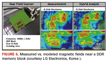
The DDR memory block of a complex PCB design is examined for emissions issues because it contains parallel buses and synchronous clocks – known to cause EMC issues. This design was characterized with system-level SI/PI hybrid analysis. The transient signals applied by the hybrid analysis were specified to correspond as closely as possible to the actual operating condition of the PCB, and cables were not considered in the hybrid analysis. Magnetic fields near the surface of the board were measured and compared to magnetic fields computed from SI/PI hybrid analysis results. The DDR board block is shown on the left portion in FIGURE 6 and the measured results are compared to the hybrid analysis results on the right. Color-shading scales are the same for the measurement.

The spatial distribution amplitude of the magnetic fields compare well between measurements and hybrid analysis. Given the engineering uncertainty of emissions, predictions are +/- 5 dB versus the typical expectations of +/- 5% for circuit design applications. This correspondence is quite adequate to assure EMC issues are well predicted by SI/PI/EMC hybrid analysis prior to manufacturing physical prototypes. Design changes can be quickly prototyped and verified with one half hour of engineering time for setup, a few hours of computer time for the analysis and 15 minutes of interactive results post processing. Government compliance specifications still must be certified by measurement for end products, but system-level PCB emissions analysis can yield a faster time to market by requiring fewer design iterations and board turns, and it can significantly reduce risks of EMC challenges when PCBs are incorporated into larger systems.
SI, PI and EMC are three sides of the same coin. It is important to recognize the relationship between SI and PI challenges, as mandated by required current loops and two-terminal voltages. In fact, SI and PI issues are indistinguishable. Similarly, SI and PI issues are the perpetrators of EMC challenges. System-level hybrid analysis is a vehicle by which these three inseparable challenges can be considered within PCB design flow. PCD&F
Brad Brim has product marketing responsibilities for Sigrity in the area of IC package and PCB extraction and can be reached at This email address is being protected from spambots. You need JavaScript enabled to view it..


