A novel soldered probe could improve access at ICT.
Test access continues to be an issue,especially for in-circuit test, which is fundamentally dependent on electrical access. One way to battle the access issue at ICT is through Bead Probe technology. This novel method is steadily becoming more mainstream, and the number of licensees increasing rapidly.
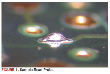
Bead Probes enable us to look at test access in a new way. A Bead Probe, which is a soldered bump (Figure 1), can be placed directly onto copper signal traces. The bumps are added using existing solder paste printing principles, reflowed using standard procedures, and then serve as the probe test point for ICT access. Beads are layout-independent (i.e., they can be added after copper layout without the need to move or modify traces) and use standard ICT methods. The bumps also merge the world of the process engineer with the test engineer – a long separate bunch of folks! This month, I explore some of the recent discoveries with using these novel bumps in a manufacturing environment. As with anything new, education, experimentation and practice will make perfect.

The bump locations need to be entered into the design. To do this, users either assign a bump location as pad geometry (normally looks like a via) or assign as a surface mount component. There are board design considerations as well. Keepout areas around components and component outlines need to be validated and respected. That said, costly re-routing of signal paths during layout to accommodate traditional test pads would not be needed. It is important to confirm the CAD denotes openings in the solder mask for the bump locations. Commercially available tools exist to automate this with no modifications to copper and with the keepouts and restrictions automatically maintained.
When doing any test and inspection, there are always CAD translation considerations to plan for. The method the layout engineer used to define the bump locations, as mentioned, needs to be known, as well as the side of the board the individual locations have been assigned. As with any utilization of CAD, being able to identify the x-y locations of the bumps will be necessary.
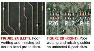
For years process engineers have studied the impact of solder paste types on printability and flux residue. Ideally the bump print deposition would be inspected using solder paste inspection or AOI to ensure print robustness and repeatability. In fact, while implementing the bump technology, users can also help identify other process issues. The photos in Figure 2, for example, are from the same board, showing obvious solder problems causing the issues noted. Flux residue on the bumps may impact contact with the probe. Minimizing residue for bump implementation is necessary and attainable with test friendly solder pastes. Process engineers have worked hand-in-hand with bare board suppliers to keep solder mask tolerances in check. These are now considerations the test engineer needs to investigate when implementing soldered bumps as well.

Fixture vendors need to be a partner in soldered bump development. Implementation has the potential to change the fixture cost. In some cases, if the bump locations are on the fixture top, costs may increase, but in turn more probing options may reduce fixture cost. Flat-faced probes are ideal. Headed or headless can be used. Headless probes permit guided probe techniques.
As with any new technology, education is critical for success. Like characterizing a new solder paste or implementing 01005 placement, process design and characterization are a must. Boning up on process engineering skills such as using test-compatible solder paste to minimize flux residue, and working with the bare board manufacturer to keep solder mask opening tolerances, will ease soldered bump implementation. Users need to work with fixture suppliers to ensure proper probe selecting and seating, which are critical. Successful implementation requires synergy among design, test, fixture, bare board and manufacturing. This synergy will provide an opportunity to opening access and in many cases provide better coverage. PCD&F
Stacy Kalisz Johnson is Americas marketing development manager at Agilent (agilent.com); This email address is being protected from spambots. You need JavaScript enabled to view it..


