by Chrys Shea, Jim Kenny, Jean Rasmussen, Girish Wable, Quyen Chu, Shiang Teng, Keith Sweatman and Kazuhiro Nogita, Ph.D.
The rate of copper dissolution in lead-free soldering may be linked to the physical characteristics of the electroplated copper.
Lead-free solder alloys, particularly those with higher silver and lower copper contents, have been shown to react with the copper on circuit boards, dissolving the copper much more quickly than tin-lead solders. Rapid dissolution of copper into tin-rich alloys can create hidden defects and reliability issues, and as copper is washed off the PCB, the exposed traces, annular rings and barrel knees can become thinner or even nonexistent.
Solid copper reacts readily with molten tin to form a layer of intermetallic compound, Cu6Sn5, at the contact surface. That is what makes tin an essential ingredient in most solders because it is that intermetallic layer that provides the metallurgical connection to ensure good electrical and thermal conductivity through the solder joint. The intermetallic compound dissolves quickly in molten tin, and as a result of these sequential dissolution processes, the underlying copper can quickly be eroded. In eutectic “63/37” SnPb solder, the inert lead diluent slows the rate of intermetallic dissolution. The effect of the lead’s presence in the eutectic SnPb is enough to slow the copper dissolution rate such that extreme copper erosion has not been a significant problem. In lead-free soldering, the high tin content (typically >95%), coupled with the absence of lead in modern lead-free solders, raises the rate of dissolution to the extent that the copper erosion occurring in normal soldering and rework processes may be sufficient to compromise the integrity of the circuit.
Under certain conditions, the copper can dissolve too fast, resulting in the removal of most - or even all - of the copper from the circuit board features. Traces and plated through holes that are exposed to wave soldering and rework processes are at a high risk for excess dissolution. Knees, the area where the barrel of the PTH meets the annular ring, are particularly susceptible to erosion problems.
The actual plated copper surface is suspected to play a part in the erosion process as well. This is indicated by the fact that two identical circuit boards from different suppliers can demonstrate vastly different dissolution properties in the same soldering process. It is believed that the dissolution rate may be affected by the grain structure of the copper because loose, open-grain structures, typically associated with columnar grain morphology, are perceived to dissolve more readily than tighter, fine, equiaxed grain structures. Generally, finer-grain structures exhibit a higher bond strength between the grains, and thus require more energy to “break” loose or dissolve.
Tensile elongation at break is an indicator of grain structure that is used as a quality assurance measure by PCB fabricators. Elongation of 16% or higher indicates good grain structure, whereas elongation in the 12% to 14% range indicates that there could be potential quality issues with the copper plating. Elongation that is less than 12% is considered unacceptable and can be a criterion for rejection. If elongation at break is an indicator of grain structure, and grain structure is a factor in dissolvability, then a relationship may exist between elongation and erodability of the electrodeposited copper.
The metallurgical properties of the copper, including tensile strength and elongation, were evaluated on plated copper to see if these characteristics could be used to determine the severity of copper dissolution during wave soldering in the lead-free environment.
Tensile Test Methodology
To perform the tensile tests, copper foil samples were conditioned at 125°C for one hour and tested in accordance with test method IPC-TM-650. Four specimens were tested from each electrodeposited sample. The requirements for acceptability of electrodeposited copper, as described by IPC-6012B, are minimum tensile strength of 248 MPa and minimum elongation of 12%.
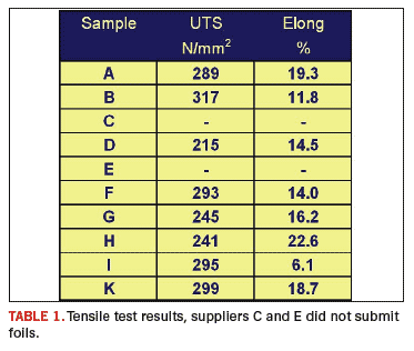
A total of 10 copper foils were evaluated. Four tensile specimens were prepared and tested from each supplier and the results were averaged. The tensile tests revealed a wide range of elongation results, ranging from 6.14% to 22.60%. The results for all samples are shown in Table 1. It should be noted that suppliers C and E did not supply foils for tensile testing.

Copper Loss Test Methodology
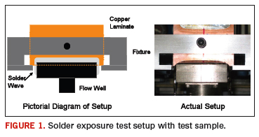
An Air-Vac PCBRM15 Selective Soldering & Rework system was used to expose the samples to flowing solder. To limit sample-to-sample variation, a fixture was built for the copper substrates to insure repeatable immersion depths and positions relative to the solder flow well. The fixture is shown in Figure 1, both before and after installation on the Air-Vac system.

Four solder alloys were tested. The first was the standard SAC alloy. Also tested were Alloy 1, a low silver SAC, Alloy 2 a SnCu with Ni solder and Alloy 3, a low silver SAC with Ni. The solder pot temperature for the SAC305 alloy was maintained at 265°C. The solder pot temperature for the alternative alloys was maintained at 270°C. All samples were processed with a solder flow setting of 6.5 on the PCBRM15 unit.
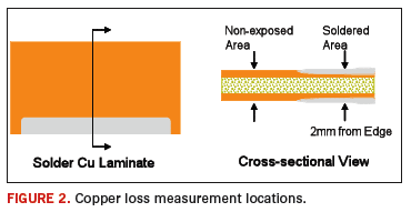
Samples were dipped in a strong, organic acid flux immediately before exposure to the solder. No preheat was used. Contact times for each alloy were determined in prescreening experiments. SAC305 and Alloy 1 used dwell times of 20, 30, 40 and 50 seconds. Alloys 2 and 3 used dwell times of 40, 60, 80 and 100 seconds. Two replicates at each of the contact times were performed. The laminate was plated on both sides, offering four data points per contact time. After the laminate samples were soldered, they were mounted and cross-sectioned. Copper thicknesses in areas that were and were not exposed to flowing solder were measured. The measurement locations are are shown in Figure 2.

Total copper loss at each contact time was measured on both sides of the test coupons and averaged. To isolate the effect of the electrodeposited copper from the laminate copper, the total loss was compared to estimates of the copper thicknesses previously recorded from cross sectional analysis. Isolation of the electrodeposited layer is important in this study because the comparison focuses on the effects of different electroplating baths.
For SAC305 at a 20-second dwell time, most of the samples demonstrated erosion in an amount approaching the electrodeposited copper thickness range; several had broken through to the laminate copper. At 30 seconds, some were still in the electrodeposited thickness range, but most had broken through to laminate copper. At 40 seconds and 50 seconds, all had broken through to laminate copper. For Alloy 1, none of the samples demonstrated break through to laminate copper at a 20-second dwell time, but several samples (one each) did show break through at 30, 40 and 50 seconds. For alloys 2 and 3, very little breakthrough to laminate copper was witnessed, even at 80- and 100-second dwell times.
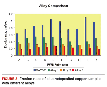
The 10 samples tested demonstrated initial erosion rates (20 second for SAC305 and Alloy 1, and 40 second for alloys 2 and 3) ranging between 0.175 µm/sec to 1.04 µm/sec, (note that for SAC305, samples C and E broke through to laminate copper, and sample K was on the borderline of break through at the 20 second data point). The details of the erosion rates can be seen in Figure 3.

Alloy 3 showed the slowest erosion rates, ranging from 0.175 µm/sec to 0.263 µm/sec. Alloy 2 was the next slowest, with erosion rates ranging from 0.263 µm/sec to 0.363 µm/sec, and Alloy 1 showed erosion rates ranging from 0.300 µm/sec to 0.538 µm/sec. These are all far lower than SAC305’s erosion rates of 0.625 µm/sec to 1.038 µm/sec. As a benchmark for comparison, Sample G was processed in eutectic tin-lead solder, and the erosion rate was 0.325 µm/sec, less than half that of SAC 305 and roughly the same as Alloys 2 and 3.
Differences in the erosion rates of the electrodeposited copper varied by a factor of 1.4 to 1.7, depending on the alloy used in the tests.
Considerable differences in the grain structures, appearances, mechanical properties and erodibility of the 10 electrodeposited copper samples were observed. While differences in the erosion rates of copper from different suppliers varied by up to a factor of 1.7, no strong correlations were identified between erosion rate, grain structure or tensile properties. Different chemistries and processing parameters may have resulted in variations in the copper structure other than the UTS and elongation that was measured. Industry experts suggests factors including grain structure, hardness or organic contamination may also influence dissolution. The work on this project will continue until the correlation factor can be identified. PCD&F
Chrys Shea is founder of Shea Engineering; This email address is being protected from spambots. You need JavaScript enabled to view it.. Jim Kenny and Jean Rasmussen are with Cookson Electronics; This email address is being protected from spambots. You need JavaScript enabled to view it. and This email address is being protected from spambots. You need JavaScript enabled to view it.. Keith Sweatman is with Nihon Superior; This email address is being protected from spambots. You need JavaScript enabled to view it.. Girish Wable and Quyen Chu are with Jabil, St. Petersburg, FL; This email address is being protected from spambots. You need JavaScript enabled to view it. and This email address is being protected from spambots. You need JavaScript enabled to view it.. Shiang Teng is at San Jose State University. Kazuhiro Nogita, Ph.D. is at University of Queensland, Australia.
Ed. Note: The experimental work contained in this article along with previously published work is part of an ongoing investigation. The complete report on current work was presented in August at SMTAI 2008 in Orlando, Proceedings.


