Improved evaluation methods clarify dielectric loss, including conductor loss and roughness loss on copper-clad laminate materials.
In recent years, more applications in the millimeter-wave band range, such as automotive radars, are being implemented. This trend is expected to continue. For a PCB to be used in these applications, it is very important that they exhibit low loss at high frequencies.
When constructing a PCB for the mm-wave range, fluoropolymer copper-clad materials are good candidates due to the extremely low-loss characteristics of the fluoropolymer material. PCBs with very small loss tangents exhibit a very low dielectric loss. On the other hand, the conductive loss will be relatively large compared to the dielectric loss, so its influence on the transmission loss will increase. Conductive loss is composed of the loss due to conductor conductivity, and the loss due to the conductor’s surface roughness. Particularly, the loss due to surface roughness increases in the high-frequency range. In this situation, it is very useful to separate the transmission loss associated with the dielectric, and the conductor loss and losses due to surface roughness to better understand the loss factors of a given substrate.
In a majority of conventional material data sheets, only the loss tangent of the material is reported. Therefore, we needed to manufacture transmission lines and measure the transmission loss in order to learn the transmission loss at the intended frequency of use and also the frequency response. Moreover, it is impossible to ascertain which substrate will present lower transmission loss using only conventional data sheets.
We measured a CBCPW (conductor backed co-planar waveguide) that is often used as a transmission line in a mm-wave band. In this work, we propose a method to separate the transmission loss into dielectric loss (Ld), conductor loss (Lc) and roughness loss (Lr). One purpose is to use the separated loss factors for developing new substrates, and another purpose is to propose the separate procedure to be better able to judge and compare the loss factors of any substrate. This allows the designer and fabricator to better compare different candidate materials.
Analytical Calculation of Transmission Loss
The calculation method for transmission loss of CBCPW is based on the impedance of CBCPW (Z0cp) and is calculated by using quasi-static analysis based on the conformal mapping method.1,2
These calculations follow where εre is the effective dielectric constant and K(*), K’(*) are the elliptic integrals of the first kind and its complement, respectively. The frequency dispersion3 and the effect of metallization thickness4 are taken into consideration in Equation 1.

Since the effect of conductor surface roughness is not considered in the above calculation, we apply Equation 2 that is based on the ratio of the rms surface roughness (Rq) and the skin depth (δ) to the loss calculation. This equation is as follows5:

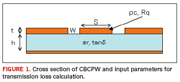
The input parameters that are necessary to calculate transmission loss are indicated in Figure 1.

There are a number of factors that can influence conductivity (ρc) and surface roughness (Rq). Plating and surface treatment of the copper conductors are major factors. Conductors, therefore, can have different conductivity depending on these treatments. To obtain the effective conductivity, the skin effect needs to be included because a homogeneous conductivity is assumed in the loss calculation. To derive the effective conductivity, one can calculate the distribution of current density in the cross section of CBCPW and the ratio of current density in each conductor using a 3D EM simulator. In modeling the effective conductivity, nickel plating followed by gold-flash plating was completed on the transmission line before measurement. It was determined, however, that the calculation associated with the gold flash need not be considered in the calculation because of the negligible effect of the thin gold coating.
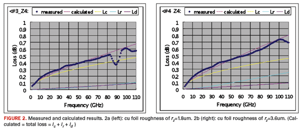
The surface roughness derived was the effective roughness from a ratio of current density on the top and the bottom of the conductor because the top and bottom surface roughness was different. It was necessary to consider the roughness of both sides and the affect to the transmission loss according to the ratio of the current density. Figure 2 shows measured and calculated results of the fluoropolymer copper clad laminate with the roughness of copper foil where Rz was 1.8µm (Figure 2a), and Rz was 3.6µm (Figure 2b).

The copper clad laminate shown in Figure 2b uses a copper foil categorized as low profile, but the roughness loss in the mm-wave band is relatively large. On the other hand, the copper clad laminate shown in Figure 2a uses a profile-free copper foil, and the roughness loss is the same level as the dielectric loss. Since the results indicated that the surface roughness of the copper foil greatly influenced the transmission loss, profile-free copper foil was used for the development of the new copper clad laminate material.
Developing Copper Clad Laminate Materials
Based on the factors above, a fluoropolymer material was developed using the profile-free copper foil (Rz is about 1µm). In addition, the fluoropolymer used had good adhesive characteristics so that it could be laminated to the profile-free copper foil without the use of a special surface treatment or additional surface roughening. The resulting peel strength is more than 1 kN/m. In contrast to conventional PTFE, the adhesive fluoropolymer allows for a completely dry process for copper-clad laminate fabrication, reducing the environmental impact of the material. It can also further reduce the process cost with the elimination of the wet-process surface preparation steps.
Transmission Loss Measurement
Transmission lines were measured on a network analyzer that could sweep continuously up to 110 GHz and was outfitted with a probe head. This measurement system provided a highly accurate measurement technique for low-loss transmission lines.
The contact pads of transmission lines are CBCPW. Maximum sequence length (MSL) was also tried as an evaluation technique for the transmission line. However, because of the transition of the influence of the line resonance, it is relatively large compared to the transmission loss in the high-frequency range. CBCPW proved to be a better method because the evaluation lines did not need transitions. The measured transmission lines were nickel and gold plated. Through-reflect-line (TRL) calibration of the network analyzer was executed, and the measurement frequency range was from 2 to 110 GHz. The length of measured lines was 8 mm.
Several transmission lines with eight different kinds of impedance were measured and analyzed up to 110 GHz in order to separate the transmission loss into dielectric loss, the conductor loss and roughness loss. Due to the mismatch with 50 ohms, the transmission loss exhibited a characteristic ripple. To compare the lines, the ripple characteristic needed to be corrected by matching with input and output impedance. After that, the measured data still showed slight ripple due to the discontinuities, and time and/or temperature drifting characteristics of the measurement system. But this minute ripple did not affect the characteristics, so it was smoothened mathematically. The above-mentioned data processing was completed, and the transmission losses of both the substrate and impedance were obtained.
Repeatability of the Measurement System
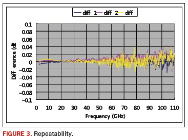
We can also confirm the repeatability of the measurement system. A transmission line was measured four times, and the difference between the raw data is shown in Figure 3. The repeatability, including the above-mentioned minute ripple, is less than +/- 0.05 dB across the entire frequency range.

For example, this repeatability is about +/- 0.02 dB in the 76 GHz range, which is the frequency of an automotive mm-wave radar system. To execute the above-mentioned smoothening, it was possible to reduce the error. Since measuring the transmission loss at that frequency is about 0.5 dB, it would appear that the measurement system has enough precision for comparing the differences between the substrates.
Measurement Results and Benchmarking
The benchmarked substrates and parameters are indicated in Table 1. The substrates, samples 1 through 4, are part of the development of the fluoropolymer copper-clad laminate. Sample 5 is the Rogers RT/Duroid 5880, and sample 6 is the major fluoropolymer copper-clad laminate material from Japan. The rms surface roughness (Rq) is the effective roughness as mentioned before. The top-side surface roughness was directly measured by stylus profilometer, and the bottom-side roughness was measured on the dielectric surface after the copper foil was etched off.

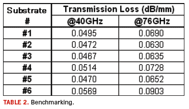
Each substrate has eight kinds of characteristic impedance (Z1, Z2, Z3, Z4, Z5, Z6, Z7, Z8) of the transmission line in descending order. We benchmarked the transmission loss average of these eight lines. The average transmission losses in the 40 GHz and 76 GHz ranges are indicated in Table 2. It was found that the transmission loss of the fluoropolymer copper clad laminate material is the same level as or less than sample 5, the Rogers RT/Duroid 5880.

Separating Transmission Loss into Dielectric and Conductive Loss
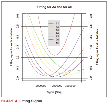
From measured transmission losses, we executed the loss separating procedure and compared the loss factors. First, we chose three kinds of impedance Z1, Z4 and Z8 from six kinds of substrate. For all the selected transmission loss factors, we added conductivity as a parameter and found the most suitable conductivity σopt. The reason that the conductivity is an adjustable parameter is because the conductivity of copper foil or nickel plating can be worse than the ideal bulk conductivity of the trace. Also, when the etching is not perfect and the conductor width is less than ideal, the loss factor is difficult to work into the calculation. For this evaluation, we used a single conductivity in the calculation for all the substrates types because all the substrates were processed through the same conditions in plating and etching, so the conductivity would be as close to identical as possible.
The surface roughness measurement was handled differently. The conductivity for each sample was uniquely identified. We factored the Rq for each material based on the surface roughness analysis of the copper foil.
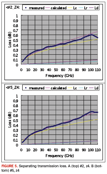
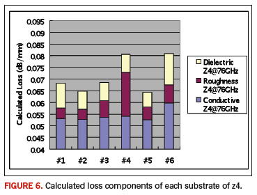
The result of fitting the conductivity is indicated in Figure 4. The “All” in the figure is the conductivity we fit to all substrates described. The respective substrates are the conductivity we fit to impedance Z4. Further, the data included 2 to 80 GHz because there was resonance in more than 80 GHz of data. Using σopt, we separated transmission loss into the loss factors as indicated in Figure 5. The loss factors for each substrate are indicated in Figure 6.

Fig. 4


In Figure 6, Sample 2 has a small roughness loss but a large dielectric loss, so the total loss is almost at the same level. This component plot clarifies the benefits of each substrate. Moreover, in a comparison of Samples 2, 3 and 4, the roughness shows the influence that gives it to the whole transmission loss clearly. Therefore, it is very useful to separate loss factors when comparing any substrate to determine the benefits of different candidate materials.
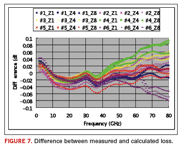
The frequency response between the actual measured and theoretically calculated results for all substrates and the three kinds of impedance are indicated in Figure 7.

It was found that the difference at 80 GHz is about +/-0.08 dB/8 mm. Therefore, since the total loss at 80 GHz is about 0.5 dB/8 mm, there is an error of about 15%. But, the trend of the difference is resembled in each substrate. The reason is that, in the calculation, the frequency dispersion of the permittivity is not applied. In future work, the dispersion of permittivity will be applied.
Conclusion
We proposed an evaluation method that clarifies not only the dielectric loss but also the conductor loss and roughness loss of copper-clad laminate materials up to 110 GHz. The impedance of CBCPW (Z0cp) is calculated by using quasi-static analysis based on the conformal mapping method. Moreover, we synthesized the effect of dispersion of the transmission line, metallization thickness and roughness for the CBCPW. Then we separated the transmission loss into the dielectric, conductor and roughness losses. It was very useful to separate loss factors. This separation is expected to improve the ability to compare the loss factors for any substrate and to allow for better determination of the benefits between different candidate materials. PCD&F
REFERENCES
1. K. C. Gupta, Ramesh Garg, Inder Bahl and Prakash Bhartia. Microstrip Lines and Slotlines, Artech House Inc., 1996.
2. G. Ghione and C. Naldi. “Parameters of Coplanar Waveguides with Lower Ground Plane,” Electron. Lett., Vol. 19, 1983, pp. 734-735.
3. G. Hasnain, et al. “Dispersion of Picosecond Pulses in Coplanar Transmission Lines,” IEEE Trans., Vol. MTT-34, 1986, pp.738-741.
4. T. Kitazawa, et al. “A Coplanar Waveguide with Thick Metal-Coating,” IEEE Trans., Vol. MTT-24, 1976, pp.604-608.
5. Marc E. Goldfarb. “Losses in GaAs Microstrip,” IEEE MTT-S International Microwave Symposium Digest 1990, pp. 563-565.
Kazuhiko Niwano, Manuel Reyes and Koji Ikawa work for Asahi Glass Co., Ltd., Kanagawa, Japan. Mitsufumi Ono works for Asahi Glass Co., Ltd., Chiba, Japan.
Ed note: This paper was previously presented and is published here with the permission of the authors.


