The amount of noise between reference planes in two adjoining
boards depends on the inductance produced by the inter-board connector.
The high-speed link paths in today’s computer systems
frequently
span across multiple circuit boards. These signal paths on multiple
boards are connected through connectors and cables, which often
introduce impedance discontinuities. The challenges presented by
multi-board signaling have been addressed in most high-speed interfaces
by using differential signaling, which is less severely impacted by
connector discontinuities. However, one pitfall of differential
signaling is the tendency to ignore the accompanying common mode signal
and mode conversion effects. Signal integrity tools often consider only
the differential-to-differential parameters (SDD11 and SDD21), ignore
other mixed mode S-parameters, and assume that the reference planes in
each circuit board are tied perfectly to a common ground. Therefore,
this kind of methodology fails to capture the common mode effects on
signals. The true scenario, however, is that at high frequencies the
reference planes in multi-board systems are independent, and therefore
significant noise voltages can develop between reference planes due to
common mode currents flowing through the connectors. This noise voltage
is a function of the common mode current and the loop inductance of the
connector as seen by the signal line. In this paper, the impact of the
non-ideal common ground on the electrical behavior of multi-board
differential signaling is studied. In particular, the amount of common
mode signal present in a realistic design, the amount of inductance
created by a signal line due to inter-board connectors, the amount of
noise between reference planes in two adjoining boards, and the overall
impact on the high speed differential signals are described.
Common Mode Signal Due to Non-Ideal Common Ground
In a multi-board system, signals are transmitted throughout the boards
using either microstrip or stripline transmission lines.
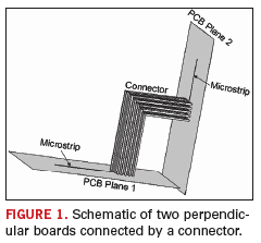
FIGURE 1
shows an example of an interface where two boards with microstrip lines
are connected through connector pins, bent at an angle that properly
connects one plane to the other. Some of the pins in the connector are
designated as the ground pins that connect to the ground planes. The
actual configuration of the ground pins will impact inductance (as
discussed in a later section) and is therefore important for the
performance of the design. In this section, the existence of common
mode noise due to non-ideal common ground connection for the example
shown in Figure 1 is demonstrated.

Measurement data proves the importance of considering non-ideal common
ground for realistic signal integrity analysis.
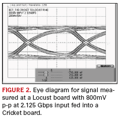
FIGURE 2
shows an eye diagram measurement obtained from a parallel bit error
rate tester (parBERT) when a 800 mV p-p differential signal is
transmitted through the device under test (DUT) at 2.125 Gbps using a
PRBS7 bit pattern. The DUT includes a driver test card attached to a
back plane through an AIRMAX connector, with a receiver test card
attached through a GBX connector. SMA cables from the parBERT generator
are attached to the driver test card SMA connectors. The SMA connectors
on the receiver test card feed into a sampling scope for capturing the
eye waveform. It can be seen from Figure 2 that the eye height is
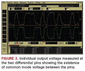
approximately 440 mV. The measured voltage waveforms, relative to
ground, on individual pins of the differential pair at the receiver
side are shown in
FIGURE
3.
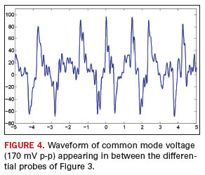
Differential receivers effectively subtract these two signals to get
the final waveform. It can be noted that the sum of the two voltages
are not zero, which indicates the presence of common mode voltage. This
common mode voltage appearing between the pins of the differential pair
at the receiver side is plotted in
FIGURE
4.
It can be seen that the peak-to-peak magnitude of the common mode
voltage is around 170 mV, which will greatly affect the signal
integrity of the multi-board system by generating ground-to-ground
noise.
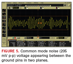
FIGURE 5
shows the
common mode noise appearing between the ground pins of the AIRMAX
connector on the driver test card and the back plane. The magnitude of
the common mode noise is about 205 mV for the 2.125 Gbps input. This
ground-to-ground noise will severely affect the signal integrity of the
design and cannot be captured using conventional signal integrity
analysis, as discussed in a later section. Therefore, it can be
concluded that the impedance discontinuity at the board interfaces,
which is conventionally ignored, must be considered for realistic
signal integrity analysis.


Modeling of PCB Connectors for Inductance Extraction
The common mode noise that appears between the ground pins in different
boards will depend on the common mode current and the loop inductance
of the signal lines at the connector. Therefore, accurate analysis and
successful design of PCBs with multiple boards connected to a main
board need to factor in the loop inductance contributed by the
connectors, which depends on the actual current return paths. Since the
common mode current flowing through the signal pin returns through the
ground pins, the separation of the signal pin from the ground pins and
their relative positioning plays an important role in determining the
loop inductance. Finding the pin configuration that minimizes
inductance is very important for PCB signal integrity. In this paper,
Partial Element Equivalent Circuit (PEEC) method, and magnetic energy
conservation method are employed to efficiently analyze inductance.
The PEEC Model.
The model of
Figure 1 is implemented in IBM’s PEEC solver, PowerPEEC.
Small
lengths of microstrip lines with a characteristic impedance of 50
Ω are used to obtain the inductance as seen by the microstrip
lines. The actual dimensions of the AIRMAX connector’s pins
are
used for modeling the DUT. Different possible configurations of the
ground pins are considered for estimating the inductance seen at the
microstrip line. Depending on the number of grounded pins and their
locations, different inductance values are obtained.
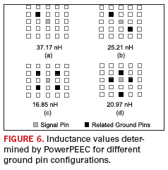
FIGURE 6
shows four possible configurations and the corresponding inductance
values as determined by PowerPEEC. The horizontal spacing of the pins
is 2 mm and vertical spacing is 1.4 mm. Note that the white pins are
considered as floating for the purpose of inductance computation. The
values of inductance show strong dependence on the ground pin
configuration, ranging between 16 nH to 37 nH for all the experiments
performed on this connector.
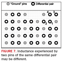
 FIGURE 7
illustrates another
important point; that the loop inductance seen at two pins of a
differential pair may vary depending on their locations. For the AIRMAX
connector used in the measurements, the loop inductance for pin 1 is
26.6 nH whereas pin 2 shows 23.6 nH. Similarly, pins 3 and 4 have loop
inductances of 31.8 nH and 28.8 nH, respectively. This will cause
propagation delay mismatch between the two leads of a differential
pair, creating more skew in the connector.

Although the results obtained by PEEC simulation will be highly
accurate, depending on the number of pins, the model size and
corresponding simulation time could be large. For example, for the
AIRMAX connector, the number of pins could be as high as 120, and the
PEEC simulation could take tens of minutes for a single ground pin
configuration, making for a time consuming search for the optimal
configuration. Therefore, a faster method of exploring different
connectors and ground configurations that also yields reasonable
accuracy should be used.
Magnetic Energy
Conservation Method.
For measuring the loop inductance caused by a connector, the method
described by Krauter and Mehrotra is found to be appropriate and
convenient. The method determines the equivalent loop inductance based
upon the conservation of magnetic energy stored in the conductor
system. For the AIRMAX connector, each pin has two segments of unequal
length – one horizontal and one vertical. For the purpose of
inductance computation, a unit current source is applied between the
horizontal terminal of the signal pin and the terminal, shorting all
horizontal terminals of the ground pins. The terminals of the vertical
portion of all pins will be considered shorted assuming quasi-static
mode.
For applying the energy-equivalence method to a system consisting of a
signal line and N ground lines, let the signal line be represented by
the subscript s and the ground lines using gi where i is the index of
the ground line. The quantities corresponding to the horizontal
(vertical) conductors will be denoted by superscript H (V). Let I be
the vector of currents flowing through each pin (with directions
signified by the sign of the current value) for unit current through
the signal pin. The partial inductance matrices for the horizontal
conductors, MH, and the vertical conductors, MV, will be given by the
following matrix considering the respective parts only:

The L terms represent the partial self inductances and the M terms the
partial If the equivalent loop inductance is Lloop, which is
the
total magnetic energy stored for unit signal pin current, then

This formulation produces a huge speedup in inductance computation
– more than four orders of magnitude – with
inductance
values within 5% of the values obtained from PowerPEEC, as shown in
Table 1.
Therefore, this formulation can be utilized for determining the optimal
ground pin configuration, quick inductance computation for signal
integrity analysis and many other applications.
Effects on Eye Diagram
The DUT that produced Figure 2 through Figure 5 is modeled for signal
integrity analysis to account for the common mode noise, which is
typically ignored in conventional signal integrity simulations. For our
simulations, the ground-to-ground noise is injected as a sine wave for
simplicity, with peak-to-peak voltage equal to the peak-to-peak ground
noise.
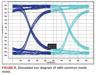
FIGURE 8
shows the
simulated eye diagram, which mimics the parBERT measurement in Figure
2, using 128 random bits simulated in a repeated fashion for 150 ns at
2.125 Gbps. The corresponding eye height is 450 mV, which is slightly
more than the value obtained by the parBERT measurement. It should be
mentioned that the effects of two 30-inch SMA cables, two 6.5-inch SMP
cables and SMA connector impedance mismatch have been ignored in the
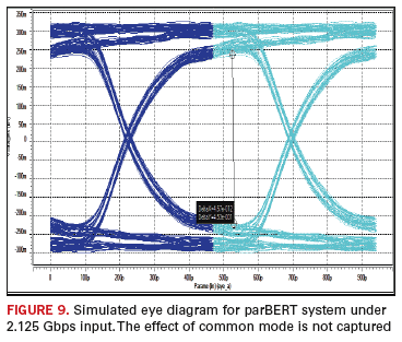
simulations. On the other hand, if the ground-to-ground noise is
ignored in the signal integrity analysis, the eye diagram of
FIGURE 9
with eye height of 510 mV is produced, which is 13% more than the
actual value. Therefore, a conventional signal integrity analysis is
unrealistic and produces optimistic results.
Conclusions
The effect of non-uniform common mode current return path on common
mode noise in high speed differential signals is demonstrated in
multi-board systems using both measured and simulated data. There are
two points to be noted. First, because of non-ideal common ground
connection, significant ground-to-ground noise appears between boards
and affects signal integrity in multi-board systems. Signal integrity
tools conventionally ignore this effect, which must be factored in for
realistic analysis and design of such systems. Second, the amount of
noise between reference planes in two adjoining boards depends on the
inductance produced by the inter-board connector. Careful choice of the
ground pin configuration can help mitigate the effect of common mode
noise.
PCD&F
Mosin Mondal
is a research assistant, ACE Lab,
Bruce
Archambeault is distinguished engineer,
Pravin Patel is
senior engineer and technical leader,
Samuel Connor is
senior engineer,
Bhyrav
Mutnury is circuit design engineer and
Moises Cases is
senior member of technical staff, all with IBM. Archambeault can be
reached at
This email address is being protected from spambots. You need JavaScript enabled to view it..
REFERENCES
1. M. Beattie and L. Pileggi, “Inductance 101: Modeling and
Extraction,” in Proc. Design Automation Conference, pp.
323–328, 2001.
2. A. E. Ruehli, “Equivalent Circuit Models for Three
Dimensional
Multiconductor Systems,” IEEE Transactions on MTT, vol. 22,
pp.
216–221, Mar. 1974.
3. B. Krauter and S. Mehrotra, “Layout Based Frequency
Dependent
Inductance and Resistance Extraction for On-Chip Interconnect Timing
Analysis,” in Proc. Design Automation Conference, pp.
303–308, 1998.
4. A. E. Ruehli, “Inductance Calculations in a Complex
Integrated
Circuit Environment,” IBM Journal of Research and
Development,
vol. 16, no, 5, pp. 470–481, 1972.


