PART 1
Successful fanout solutions provide escape routing for a
combination of serial and parallel nets.
The
effectiveness of a fanout pattern on large BGAs contributes
significantly to the route-ability of a design, which impacts the layer
count and affects the cost of the board fabrication. The fanout of a
BGA is only a part of the routing solution, which may also include
escape traces and general interconnect routing of the pins. The goal of
the BGA fanout effort should be to eliminate the BGA routing as the
primary contributor to increasing layer count while maintaining signal
integrity and fabrication yield requirements.
In a
theoretical approach to BGA breakout, the BGA is analyzed outside the
context of a real design. This kind of solution is a mathematical
excercise in layer reduction that makes unrealistic assumptions and
disregards SI requirements.
Unfortunately, reality
requires much more than just a mathematical solution. Deriving fanout
patterns in a theoretical realm can actually be fairly simple, but
finding effective fanout patterns when all the design and packaging
challenges must be considered is a much more difficult problem.
It
would be ideal to have power and ground pins only in the center of a
BGA, however, power integrity requires they also be distributed among
the signal pins. This distribution is rarely in neat columns and rows,
which would open up considerable routing space.
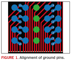
Figure 1
shows an ideal distribution of ground pins (green). If the BGA had
ground pins aligned this way, and if the mount layer was a GND plane,
then you would see additional room made available on the inner routing
layers.

Unfortunately, most FPGA
vendors distribute the power and ground pins around the BGA or use some
pattern other than columns and rows. The purpose of distributing power
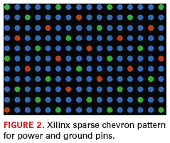
and ground pins is to improve the power integrity. Xilinx often uses a
“Sparse Chevron” pattern as shown in Figure
2. In this figure the ground pins are green and the
power pins are brown.

There
may be some ASICs that have power and ground pins aligned in columns
and rows, however, such an ideal condition is not common, and therefore
effective fanout and routing solutions must incorporate other ways to
reduce the layer count.
Most large BGAs have a
combination of serial and parallel nets that must be routed as
differential pairs and single-ended nets (respectively). Some FPGAs
also allow for nets to be programmed as either serial or parallel.
These devices support multiple I/O performance standards that could
require differential routing.
Differential pairs and
single-ended nets require different trace widths and spacing to
maintain desired impedance, and although it is possible to use the same
spacing rules inside the BGA area, impedance discontinuity may become
significant in some high-speed circuits.
For example,
it is common to have a target of 50 Ω for single-ended nets
and 100 Ω
for differential pairs. Of course the stack up thicknesses and
materials will affect the impedance; yet it is common to see a 0.15 mm
(6th) for differential pair spacing while single-ended nets can have
0.1 mm (4th). Actual trace widths and clearances will vary depending on
the specific high-speed and fabrication requirements for each design.
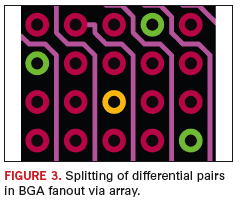
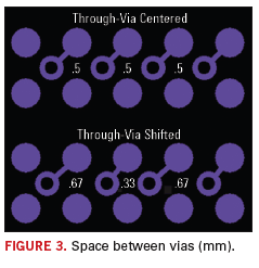
If
the fanouts are positioned such that differential pairs need to be
split to maintain the trace width and clearance rules, that could also
cause significant signal integrity problems, as illustrated in Figure
3.

Summarizing,
a theoretical fanout and breakout solution that does not take into
consideration the potential for varied trace widths and clearances is
not very useful. The problem becomes even more difficult when each I/O
pin or bank of pins can be programmed to require either differential
pair or single-ended routing.
An effective fanout
solution that enables the most efficient escape routing should be
flexible enough to support the trace width and clearance requirements
for a mixture of serial and parallel nets.
PART 2
Through-vias provide the lowest fabrication cost but can
limit routing density.
This is the fourth in a series of articles on BGA routing methods. My
objective is to reveal the routing problems often associated with large
pin-count BGAs, and provide the PCB designer with effective techniques
that enable higher route density and reduction of layer count.
Through-Vias
There are not many fanout options,
due to the large via pad relative to the 1-mm ball pitch. Either a
“Quadrant Dog-Bone” or
“Via-in-Pad” method is appropriate.
Theory: Removing Vias
One
method proposed to increase route channels on inner layers is not to
use fanout vias where possible, for power, ground and unused pins. When
using through-vias, there is very little benefit in not adding fanout
vias for the 30% to 50% of the BGA pins that will likely be assigned to
power, ground or unused. The power and ground pins will be assigned to
the center of the device and distributed among the other pins. It is
highly unlikely that they, or any unused pins will be distributed in
columns and rows.
When using through-vias for
fanouts, rather than trying to gain a few route channels by eliminating
connections to the planes, it is best to gain the power integrity
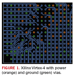
benefits by adding fanouts for all power and ground pins. In Figure
1,
it is clear that the vias for power and ground are scattered such that
even if they were removed, little would be gained. The outer perimeter
of through-vias dictates the space available for routing, and at least
in the case of the Virtex-4, few of them are assigned to power and
ground.

If an ASIC can be
packaged to provide adequate power integrity and have the power and
ground pins aligned in such a manner so as to increase route channels
(by not using fanout vias) that would be a good design, but this is
likely to be a rare occurrence.
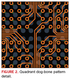
Quadrant Dog-Bone
This fanout pattern has the fanout vias in the center spaced
between the ball pads, and angled in one of four directions.
Advantages over via-in-pad.
- It
opens up additional routing channels in the center row and column,
giving room for two or three more routes per layer, which could
contribute layer reduction, seen in Figure 2.
- On
the side of the board opposite the BGA mount, the column and row
channel gives a convenient place to add capacitors and pull-up
resistors.
- A lower cost and less risk of soldering problems related to
the via-in-pad.

Disadvantages over via-in-pad.
- When using a ground or power plane on the BGA mount side,
the fanout via pads prevent a continuous plane fill under the BGA.
Shifting Through-Vias
Choosing
to place the fanout via outside the center of the ball pad array has a
relatively little benefit to routing due to the lack of space. Any
benefits depend on the design rules. You could move the vias off-center
somewhat in order to form columns and rows, but for every additional
route channel opened on one side, it will close a route channel on the
other – the net result being the same number of route
channels across
the entire BGA.
However, if the design rules are
such that differential pairs cannot be routed together between the
through-vias, and a little more space is required, then shifting
through-vias slightly might make sense.
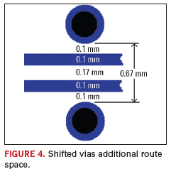
In Figure 3 and Figure
4,
note that by shifting the vias to the left on one column and to the
right on the next column, you gain 0.17 mm in one and lose 0.17 mm in
the other. These values could vary, depending on your ball pad size and
clearance rules. This option might be useful if you have some critical
signals that require greater spacing within the BGA breakout area.


Another
reason for shifting through-vias while using Quad Dog-Bone patterns is
to maximize the amount of plane fill on the mount layer. Again, any
benefit is dependent on the design rules.
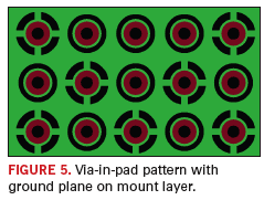
Via-in-Pad
This pattern has a simple solution, which is to add a
through-via in the center of each of the desired BGA ball pads as seen
in Figure 5.

Advantages over quadrant dog-bone.
- If you have a ground or power plane on the BGA mount side,
the fanout via pads allow a continuous plane fill under the BGA.
- If
you do not use the mount layer for a plane, then you have an additional
routing layer for the BGA – albeit a surface layer, which may
cause
impedance problems when using high-speed nets.
Disadvantages over quadrant dog-bone.
- There are no additional route channels in the center column
and row.
- There is less room for capacitors and resistors on the
opposite side under the BGA, since the fanout via array is full.
If the BGA has unused pins and you do not add fanout vias for
them, there will be available room for components.
- There will be a slightly higher cost for filling the vias
and ensuring a smooth surface when soldering the ball pads.
- There
is some risk of BGA soldering problems (delamination or pop corning)
with via-in-pad when using lead-free solder. An experienced assembly
company should be able to manage this risk.
Better Methods
Although
through-via stackups generally provide the lowest cost fabrication, the
large size of the via severely limits your ability to maximize route
density and therefore leads to excessive layer count. The next article
will clearly demonstrate the benefits of using blind and buried vias.
PART 3
Aligning blind via fanout patterns can significantly increase
route density.
We
have already come to the fifth article in this series on BGA breakout
and routing methods. Those who have been following along have read
about unusual and upcoming packages, theoretical breakout solutions,
and the limited set options when using through-via fanout patterns. The
intent in all these articles is to provide ideas and methods that will
enable greater route density for BGAs, resulting in fewer layers while
still maintaining signal and power integrity.
Blind and Buried Fanouts
The
basic principles for effectively using fanout patterns can be applied
when using blind and buried vias, even in a laminated stackup. Although
the via sizes are still larger than in an HDI stackup using micro-vias,
the blind and buried vias are still small enough to obtain significant
route density gains.
Shifting Vias
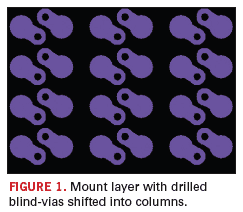
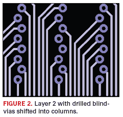
In Figure 1, the blind-vias have
been shifted into columns with the intent of opening up additional
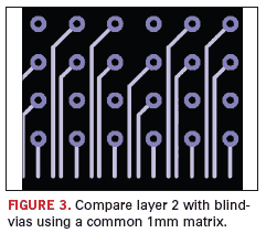
routing space. In Figure 2, you can see
that significant space is created as compared to the unshifted pattern
in Figure 3. Figure 2 shows how shifting
the vias can add an additional 24% increase in the number of escape
traces at the edge of the BGA.


Observe
that the blind vias are not in a straight column because via size and
via-to-via clearance (0.1mm) forces them to be staggered.
The advantages of shifting vias include:
- 24% increased route density per layer over through-vias and
unshifted blind vias.
- More room for a ground plane on the mount layer (but not as
much room as with via-in-pad).
- If
you route the high-speed single-ended nets on the layers using blind
vias, via stubs are eliminated and via-to-via crosstalk is minimized.
- Any
signal routed on the blind via layers will not need to have a buried
via, thus opening up route space on the buried via layers as well.
The disadvantage is that blind and buried via stackup is
slightly more expensive than a through-via stackup.
As
shown above with blind vias, it is clear that shifting the via position
can increase route density. When using HDI microvias, shifting the
fanout locations can improve route density even more. Increased route
density means potentially fewer layers and lower cost. There are some
general principles related to shifting vias that can help make the
effort successful.
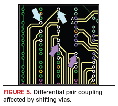
Differential Pair Coupling and Pin Swapping
When
applying a shifted via pattern in order to increase route density, one
of the results that will possibly need to be managed is that as the
transition progresses through the layers with different patterns in the
via span, the differential pair compliments may be moved away from each
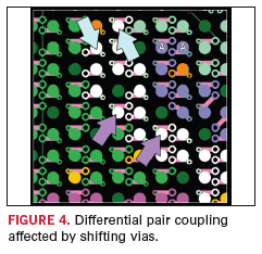
other. Figures 4 and 5
illustrate
this problem. The ball pads for the differential pair compliments may
be designed in the FPGA or ASIC to be placed closely to each other, but
as fanout vias are added, the compliments may end up further apart than
originally intended.


A
good solution, especially for FPGAs, is to pin swap, so that the ball
pads are aligned in a manner that allows the fanout vias to remain
close to each other. In Figures 4 and 5, swapping the differential pair
compliments into the “A” and
“A” locations will optimize the coupling.
The
ability to swap pins will be limited by bank locations, differential
pair or single-ended pin assignments, and power and ground pin
distribution. Finding the most effective swapping patterns (aligned
vertically, horizontally, or on a diagonal) will depend on the fanout
via pattern used in that area.
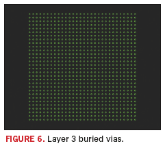
Reducing the Effective Size of the BGA
If
the ball pads around the perimeter can be fanned-out and routed on the
blind via layer (layer 2), then the effective size of the BGA routed on
the buried-via layers (Figure 6) will
become 1024.
With that number of pins, breakout and routing of the BGA is no longer
the primary contributor to layer count, especially since the innermost
pins in most BGAs are usually dedicated to power and ground.

Principles
Aligning
blind via fanouts in well-organized patterns can significantly increase
route density on those layers where it is incorporated. Increased route
density means that more rows of ball pads around the perimeter can be
routed on the blind via layers, which will result in effectively
decreasing the size of the BGA routed on the buried via layers.
PART 4
Creating effective fanout patterns for microvias in an HDI
stackup.
HDI microvia fanouts for laser drilled micro-via stackups use the same
principles as mechanically drilled blind and buried vias. The variety
of stackups and smaller via sizes provide for tighter shifted column
and row patterns, improved route density and greater flexibility in
assigning routes to buildup layers than does standard laminated cores.
When using HDI, the blind micro-vias allow for greater route density,
and therefore potentially fewer total layers required for routing. Of
course, the number of layers accessible by the micro-vias will
significantly affect the overall route density. The fanout patterns
analyzed in this context will be for the following types of HDI
construction:
1+N+1 = Type II (Layer 1:2 microvias with buried vias in a laminated
core)
2+N+2 = Type III (Layer 1:2, 2 to 3 microvias with buried vias in a
laminated core)
Layer 1:2 microvias (1+N+1)
If Layer 1 is used for a ground plane and not for routing, then the
fanouts need to be patterned to maximize Layer 2 route density. The
same patterns described in the previous month’s article for
blind
vias can be used for microvias, however, since the microvias are
smaller, they can be further compacted to gain additional route space.
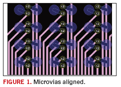
In
Figure 1,
the 1:2 microvias
are aligned in columns to maximize route density (12% improvement over
shifted blind vias, 36% improvement over quadrant dog-bone through
vias.) It is easy to see how route density can be increased
when
using via-in-pad methods.

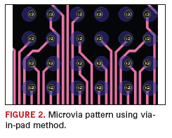
If the vias are shifted inside the pads as shown in
Figure 2, you can
open up additional room for the escape traces.
If only one layer is available for the escape traces, as is the case
with a 1+N+1 stackup that has a ground plane on the surface layer, then
it is important to use a shifted via pattern that is allows for aligned
microvias around the BGA perimeter. This will allow space for the power
and ground to extend through the board using additional buried and
blind vias.

Layer 1:2, 2 to 3 microvias (2+N+2)
Again, assuming that Layer 1 will be a ground plane, then the fanouts
need to be patterned to maximize the Layer 2 and Layer 3 route density.
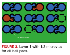
Figure 3 and
Figure 4
show how effective the general principle of aligning vias works to open
additional route space on inner layers. Figure 3 shows that the
shifting of vias not only provides additional route density, but it
also opens space for uninterrupted ground fill. Also note how nicely
the ground via fits, and the how the copper fill and clearance around
it provides for ease of manufacturing. The thermal relief ties are also
rotated off the 45-degree center, to maximize the connectivity and make
room for the nearby fanout via.


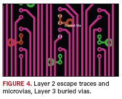
In
Figure 4,
note the
significant space for routes after shifting the vias. In this case, the
traces are routed as single-ended nets, however, if the nets were
differential pairs, there would be plenty of room to route three sets
of differential pairs between the aligned vias. Of course, practical
applications such as these may vary depending on design rules.
The power (orange) and ground (green) vias are paired because both the
1:2 vias, but also the 2:3 vias can be seen on Layer 2. Observe as well
the wide-open space for traces on Layer 3, where the buried via
starts.Results may vary depending on actual design rules. In the above
examples, the trace widths are 0.1mm/4th and the via pad size is
0.254mm/10th.
Effective fanout patterns can significantly increase route density.
Designs with through vias under BGAs have limited options, but by using
laminated blind vias, route density can be increased 24%, and using HDI
micro-vias allows a 36% increase in route density.
These four articles on fanout patterns clearly show that aligning
blind-vias or micro-vias is a very effective method for potential layer
reduction through increased route density.
The next article will present a new concept for organizing multiple via
patterns for a single BGA, and the positive impact it has on increasing
route density.
PCD&F
Charles Pfeil
is an engineering director for Mentor Graphics, Systems Design
Division; This email address is being protected from spambots. You need JavaScript enabled to view it.; mentor.com/pcb. He has authored a
book, BGA Breakouts and
Routing, which explores in greater detail the
content of this column. Please visit mentor.com/go/bga to order a copy.


