Dynamic new co-design strategies will give the PCB designer the flexibility to re-map legacy package pinouts.
The approach to IC chip packaging design has remained fundamentally
unchanged since the 1970s. The chip design team lays out the silicon
die and decides what type of IC package to use and how to assign the
pinouts. While efforts continue to make co-design of electronic
assemblies a reality, no clear communication channel presently exists
between the chip and PCB design teams. IC packages are, as the saying
goes, simply “tossed over-the-wall” to board designers who are left to
deal with whatever comes their way. This is a condition that might well
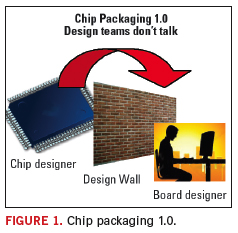
be called “Chip Packaging 1.0” (Figure 1). Since the
IC package pinouts are documented in the chipmaker’s datasheet, the
board designer has no ability to change any aspect of the IC package or
to re-map the pinout when necessary. As a result, the board designer
has his shoelaces tied when he enters the race to design his product.

In
spite of the recent hoopla to bring co-design into the mainstream, the
long-standing protocol of IC design may never entirely go away.
However, improvements are possible if IC packaging adopts a new
approach that offers more design freedom in what might be codified as
the “Chip Packaging 2.0” environment. This new approach is compelling
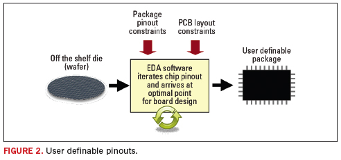
and worthy of consideration. In the new approach, the PCB designer will
use their EDA software to iterate the IC package pinouts of a legacy IC
die while simultaneously optimizing the board’s routing (Figure 2).
This new approach to semiconductor packaging is descriptively referred
to as “User Definable Pinout” (UDPo), which enables designers to re-map
package pinouts of legacy chips using EDA software tools. The optimized
chip is wired by the chipmaker according to the pinout instructions of
the PCB designer and added to the PCB BOM for assembly using normal SMT
assembly practices.

In looking at a circuit board’s
initial design process, the board designer typically makes a series of
tradeoffs between electrical, thermal and mechanical needs. Once
component locations are established, the circuit schematic is loaded
and autorouting of the board commences. The iteration process begins by
benchmarking the initials results achieved with “standard pinout”
packages. Next, the EDA software begins the pinout iteration process,
and pairs of pinouts on selected IC packages are processed while board
routing is observed. During the iterative process, improvement is
observed as copper routing is shortened, board size is reduced and/or
fewer inner layers are required. Circuit speed improves roughly one
nanosecond in a theoretical lossless substrate for each 6-inch (150 mm)
reduction of dual copper path (signal plus ground) according to the
speed of light formula.
Typically, the pinout of
one chip at a time is optimized, then cycled to the next chip until the
total circuit board is optimized to the satisfaction of the board
designer. Once the chip pinouts are optimized, the EDA software will
output a bonding schedule (net list) for input into wire-bonding
machines. The chip packages are bonded using insulated bonding wire, an
important feature of this new approach, to prevent shorting inside the
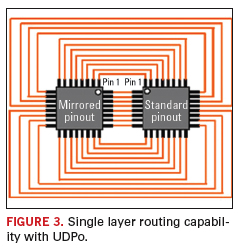
IC package. Once optimized, there is even the possibility of creating
single layer boards as shown in Figure 3.

Design Issues with UDPo
While
there are a number of promising attributes in the ideas being proposed,
there are also many issues to be solved before Chip Packaging 2.0 can
be adopted as a standard industry practice.
For
example, EDA software tools to optimize chip pinouts must be both
reliable and economical before mainstream board designers will adopt
them. There are already efforts being made along these lines, with
several companies working on EDA chip co-design and optimization
software. Some of these tools were demonstrated during the 2007 Design
Automation Conference (DAC) in San Diego and the 2007 Semicon West show
in San Francisco.
Assuming that the aforementioned
issues with EDA software are resolved, the next challenge for the UDPo
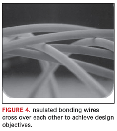
approach is in assembling die that may have cross-over wire bonding.
Traditional wire bonding is very neat and orderly, however, in the
proposed environment “neat and orderly” may need to be replaced with
visually disorderly wires that cross over each other (like the type
manufactured by Microbonds X-Wire insulated bonding wire) in order to
achieve design objectives (see Figure 4).

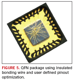
Most wire bonding machines are easily converted to use insulated bonding wire. Figure 5 shows an extreme example of insulated bonding wire used in an open cavity QFN package.

Industry
standard JEDEC IC package outlines such as QFN, QFP, SOIC, BGA, CSP,
TSOP are all easily adapted to the concept of UDPo.
When
using bonding wires, the cumulative thickness of crossing wires cannot
exceed the maximum “headroom” of the IC package, which is approximately
10 mils between the upper most wire and the internal ceiling of the
plastic IC package. Assuming that typical insulated bonding wire is
1mil in diameter, the maximum number of crossing wires is easily
calculable by the designer, while also allowing for the thickness of
the die and the lead frame.
The Economics of Designing with User Defined Pinouts
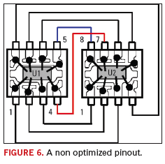
A very simple circuit design will help to illustrate how this new UDPo approach can improve design. Figure 6 illustrates
the “before” non-optimized board design. U1 and U2 are off-the-shelf
8-pin SOIC packages. The copper routing on the PCB from U1-pin 4 to
U2-pin 7 crosses the copper routing from U1-pin 5 to U2-pin 8. To
prevent short circuits, board designers would typically add a layer
with plated vias to complete the design.

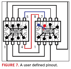
For comparison, Figure 7
illustrates the “after” “optimized” board, with improvements achieved
by simply re-mapping the pinouts of U2 without changing the performance
of the silicon die. The optimized board has shorter copper routing,
less plated vias and fewer layers.

The board designer
can thus use EDA chip pinout optimization software to simultaneously
iterate and re-map U2, while auto-routing copper traces on the board.
After completing the iteration process, the EDA software indicated that
2 bonding wires inside U2 should be remapped, using bonding wires from
die pad 7 to lead-frame pin 8 and from die pad 8 to lead-frame pin 7.
The
EDA software then creates a bonding schedule (net list), and the data
is presented to IC packaging fabricators to assemble the legacy die (or
wafer). The wire-bonding machine employs insulated bonding wire to
prevent short circuits with the chip package, and U2 is then sent to
the board assembler who uses standard SMT assembly practices to mount
components and complete the board assembly. Though the above examples
in Figure 6 and Figure 7 are simple ones, the same processes can be
applied to complex board designs.
It is anticipated
that in the early stage of UDPo design, cost per device will be higher
due to low volume, non-recurring development and device testing costs.
However, it is likely that these higher costs could easily be offset by
the lower material costs in PCBs using this design method (smaller
boards, fewer inner layers, smaller cabinetry, etc.) as well as the
benefits of a faster time to market. Since resultant board designs will
become simpler, it is anticipated that there will also be a lowering of
costs related to improved yields, reduced testing and rework and lower
field failure rates.
Summary
The
UDPo approach to co-design, which begins design at the IC package
itself, is a dynamic new technique for printed circuit board designers,
allowing them to optimize board-level designs by actually re-mapping
pinouts of legacy die. In the current packaging environment, there is
no communication channel for chip designers to collaborate with board
designers, and it need not be that way in the future.
The
old “throw it over the wall” approach to IC/PCB design has reached its
practical limits. One solution is to give tools to PCB designers that
facilitate their ability to re-map legacy package pinouts without
changing the performance of the silicon. With this type of tool, PCB
designs could be better optimized using IC pinout co-design techniques.
Suitable
EDA software that can re-map legacy chip pinouts while simultaneously
optimizing the board, create a requisite chip pinout-bonding schedule,
and seamlessly deliver it to wire bonding machines (via the Internet or
by conventional means) will be needed to reap the prospective benefits
that await. PCD&F
Martin Hart is founder and CEO of Mirror Semiconductor. For more information, contact This email address is being protected from spambots. You need JavaScript enabled to view it..
Acknowledgements
My gratitude to Joseph Fjelstad for reviewing the manuscript and furnishing excellent feedback.


