An interview with Chantal Holloway and Guillaume Turgeon – two of the
2007 winners of the Mentor Graphics PCB Technology Leadership Awards.
Category: Industrial control, instrumentation, security & medical.
Company Name: Gage Applied Technologies Inc.
Designers: Chantal Holloway, Guillaume Turgeon
Design Description: High-speed mixed signal board.
The
PCB Technology Leadership Awards have been around for 20 years, and
provide PCB designers with an opportunity to have their best designs
judged by a panel of experts. The categories included:
- PC Computers and Peripherals
- Consumer Electronics & Handhelds
- Industrial Control, Instrumentation, Security & Medical
- Military & Aerospace
- Telecommunication Switches, Network Servers, Base Stations and Computer Mainframes
- Transportation and Automotive
There is also an award for best overall design.
In
2007 designers came from around the world to participate, heralding
from Germany, Switzerland, China, Norway, Singapore, Austria, Canada,
Korea, India, Israel, Portugal, the United States and the United
Kingdom.
The design team of Holloway and Turgeon took
the gold in the industrial control, instrumentation, security and
medical division. Their design, a high-speed mixed signal board with
both electrical and mechanicals constraints, resulted in a 12-layer
stack up with split and mixed signal planes. In order to optimize the
opposing requirements of the analog and digital sections of the PCB, it
was necessary to develop a split plane and routing plan that addressed
potential cross talk between the PCB domains.
The
original design challenge was to upgrade the PCB for improved
performance while lowering the cost. The previous design had used two
stacked PCBs joined by a connector. The new single PCB surpassed the
targeted design parameters. It will be manufactured at a lower cost
than the previous two board design, accommodated a higher sampling rate
digitizer, ran at higher speeds than expected, and had lower power
consumption.
The challenges included designing two
different products, one that would be used in an add-on board
configuration and one that would be a stand-alone design. There were
considerable high-speed analog front-end constraints. Routing was
particularly difficult, with matched length differential pairs and 452
high-speed nets. Gage used a new design tool, specifically developed
for high speed routing, to manage the difficulties of routing CLK
signals, differential pairs, and high-speed signals.
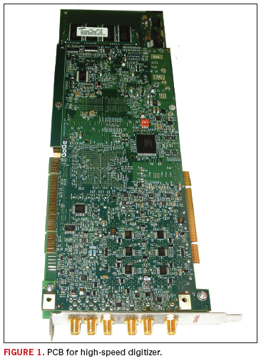
A photo of the PCB can be seen in Figure 1.
One of the main challenges with this design was the requirement that a
single PCB would be used to accommodate different final product
configurations. This feature is customized during the assembly phase.
The design used two duplicate Master/ Slave interfaces to accommodate
standalone PCI or baseboard connection. This places some restrictions
on component placement.

- The board statistics are as follows:
- Board Dimensions: 9.633 x 3.55 inches
- Board Thickness: 0.062 inch
- Usage Area: 34.19715 inches
- Laminate Material: Polyclad 370HR RoHS Compliant for Lead Free Assembly
- Total Number of Layers: 12
- Number of Signal Layers: 8
- Number of Power Planes: 4
- Minimum Spacing: 4.25 mils
- Minimum Line Width: 3.75 mils
- Minimum Vias Size: 10 mils
- Minimum Pad Size: 19 mils
- Number of Vias: 3,983
- Number of High-Speed Nets: 452
- Number of Pin-to-Pin Connections: 7,445
- Component Placement: Double-sided
- Number of Components: 2,253
- Total Component Area: 668.00
- Number of Component Pins: 9,353
- Minimum Pitch: 0.5 mm
- Component Complexity: up to 1,020 pin BGA
When
asked about the most challenging aspects of the design, Holloway and
Turgeon responded, “One main challenge of this board was to accommodate
different final product configurations utilizing a single PCB layout.”
They continued, “A minimum trace length in addition to matched length
routing strategy was used for the DDR-II Interface between the high
density BGAS and the SODIMM to the termination resistors.” Same length
matched routing from the SODIMM attached to the baseboard connector
provided one configuration. A component free area 1.300 x 2.500 inch
for memory module insertion accommodated the second configuration.
The
end product is a next generation high-speed digitizer. The flexibility
provided by the reconfigurable PCB allows for one or two channel
sampling at rates up to 3.2 GS/s. With the product name Rabbit, this
digitizer, made possible by the PCB design excellence of the Holloway
and Turgeon team, promises to make a significant impact on the market
with its higher speed and larger sampling capability. PCD&F
Kathy Nargi-Toth is editor of Printed Circuit Design & Fab.


