When using differential circuits, specific design rules can maximize the advantages while minimizing design-induced difficulties.
As the PCB industry moves toward designing faster and more miniaturized
products, data rates are constantly increasing, and printed circuits
are shrinking. The need for transmitting the signals cleanly from the
driver to the receiver has become of prime importance and has increased
the need for using differential signaling.
Differential signals involve a pair of traces routed at a uniform
distance from each other over its length. One trace carries the
positive signal while the other carries the signal that is equal, but
opposite in polarity.
Differential signaling is not new. It has been around ever since the
existence of large-scale computing to move logic signals from one
circuit to another. The only hindrance to its extensive use is the fact
that every differential signal requires two wires, a set of drivers and
a set of receivers. Hence, it is used for signals that require greater
immunity to noise, or if the data rates are high and there is a ground
offset between the driver and the receiver. However, if certain design
rules are not followed, the functionality of the circuit board may be
affected. This article describes the different applications of
differential signaling and the correct way to implement them.

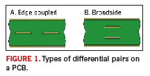
On a PCB, differential signals can be implemented in two ways, as shown in
Figures 1a and
1b. In these figures:
- Edge coupled: The differential traces are routed side by side.
- Broad side: The traces are routed one over each other on consecutive layers.
In nine out of 10 cases, edge coupled differential pairs would be used, primarily for two reasons:
- Lack of control in maintaining uniform dielectric thicknesses.
- Single-ended impedance mismatch between each member of the broadside differential pair.
Differential Signal Applications
To correctly implement differential signals on a PCB, a designer must
first know the main reason behind using differential signals. The main
advantages of using differential circuits are as follows.
Once a differential signal is transmitted and the receiver picks up the
signals, it calculates the voltage difference between the two positive
and negative signals. Hence, the received voltage is effectively
doubled. This facet is very useful for low-level applications where
signal to noise ratio is a problem, e.g. LVDS.
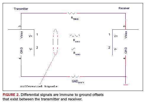
The second advantage is that once the receiver compares the two signals
to determine their logic polarity, the task does not require any
reference voltage. Hence, the differential reception is unaffected by
ground voltage shifts between the transmitter and receiver, as shown in
Figure 2. Consequently, the differential circuits are capable of
dealing with significant ground offsets that exist between the two ends
of the data path.

Another advantage is that there is no need to provide a low impedance
path to the return, since there is none. This is because the returns of
both the +ve and the –ve signals nullify each other. Hence, during
layout of a mixed-signal PCB, if an analog signal is transmitted as a
differential signal to a digital device, there will be no problem if
the signal crosses power planes.
The fourth benefit brought about by using differential circuits is that
these signals are fairly immune to outside EMI and crosstalk from
nearby signals. This is because: the received voltage is being doubled,
and theoretically, the noise affects the tightly coupled traces
equally. Therefore, they cancel each other out.
In addition to being less susceptible to interference, differential
signals also tend to produce less EMI. This is because the changes in
signal levels (dV/dt or dI/dt) create opposing magnetic fields, again
canceling each other out.
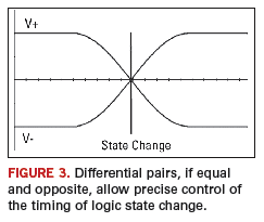
Another benefit provided by differential signaling is the ability to
control switching timing more precisely. Remember, that for the
single-ended signals, the return currents are on an imaginary path on a
reference plane. For these signals, the crossover point is either a one
or a zero, which is subject to crosstalk or outside EMI. Since the
differential pairs are referenced to each other, and the pair is routed
as equal and opposite, it brings about a more precisely controlled
crossover point, as shown in
Figure 3.

Differential Signal Design Rules
When the differential signal is launched from the cable to the PCB,
interconnections may cause problems at high speeds because of impedance
discontinuities that exist between the cable, connector or the board.
Specialized connectors are used with proper shielding. Special
modeling, simulation and measurement validation are required to ensure
a smooth transition of the signal from the cable to the trace.
Once this transition has been taken care of, the signal comes under the
domain of the layout designer, and it is his or her responsibility to
ensure its signal integrity. There are some rules that need to be
followed while implementing differential signals.
Rule # 1: The differential traces in a pair need to be of an equal length.
This rule originated from the fact that a differential receiver will
detect the time at which the negative and positive signals cross each
other – the crossover point. Hence, the signals should arrive at the
receiver at the same time for its proper operation. For this reason,
the traces need to be equal in length.
Recent studies have shown that differential circuits can tolerate
switching timing, and hence, the length mismatch to a great deal, and
will show little or no jitter. In fact, many people would go to the
length of declaring it a myth. They fail to understand, however, that
switching timing is just one of the reasons why differential signals
are maintained at equal lengths. If there are high-speed differential
signals that are not exactly equal, then their return currents will not
cancel each other, and there may be high-speed currents on one of the
planes that are unaccounted for. These currents can create serious
problems such as EMI and crosstalk for other circuits.
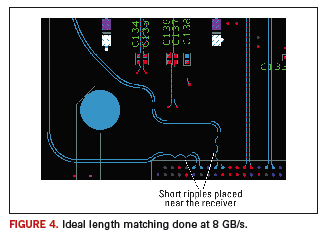
Figure 4 shows
one way of maintaining an equal length for a high-speed differential
signal. Note that the ripples are placed near the receiver where the
source of length imbalance lies.

Rule #2: The traces within a differential pair need to be routed as close as possible.
This rule is based upon the fact that since the differential signals
are equal and opposite, and if external noise equally interferes with
these signals, it (the noise) should nullify. Similarly, any unwanted
noise induced by the differential signals into adjacent conductors
should cancel each other out if traces are routed side by side.
However, if the signals do not have fast rise times, then side-by-side
routing becomes comparatively unimportant. Furthermore, sometimes
designers fail to understand that there exists some destructive
coupling within the differential signals, which is inversely
proportional to the distance between the traces. Moreover, the closer
the traces are to each other, the lower will be the effective
impedance, and maintaining the original impedance will require reducing
trace widths or adjusting the termination schemes.
Rule #3: The trace separation within a differential pair needs to be constant over its entire length.
The main reason behind this rule is Rule #2. If the differential traces
are routed close together, then they are impacting the overall
impedance. Now if this separation is not maintained all the way from
the driver to the receiver, there will be impedance mismatches along
the way, resulting in reflections.
Differential Impedance Calculations
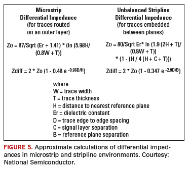
The impedance of edge coupled differential signals depends on the following factors:
-
Zo: Impedance of the single-ended trace
- Differential trace width and thicknesses
-
Differential air gap
-
Height of each trace from the plane
-
Dielectric constants of the media.
The differential impedance can be calculated by the formula shown in
Figure 5.

Conclusion
Differential signaling has been around for a long time, and there is
very little chance of it disappearing from the PCB design scene. It is
imperative for both design and layout engineers to fully understand the
concepts behind the need for differential circuits and the proper
design rules, which if not followed correctly, will diminish their
advantages and may even create more problems for the rest of the
circuit.
PCD&F
Syed W. Ali, C.I.D, is a PCB layout engineer with Nexlogic Technologies Inc., San Jose, CA;
This email address is being protected from spambots. You need JavaScript enabled to view it., 408-436-8150.
Bibliography
Brooks, Douglas. I
ntegrity Issues and Printed Circuit Board Design.
Lattice Semiconductor Corp. “Differential Signaling,” AN6019. May 2001.
National Semiconductor. “Transmission Line RAPIDESIGNER Operation and Applications Guide.” AN905. May 1996.
Ritchey, Lee W.
Right the First Time, Volume One.


