Approximating loop inductance can point out the design features that best lower inductance in the power-return path.
While
inductance is one of the most confusing topics in signal integrity,
and, in general, difficult to calculate, there is a special case that
is easy to understand and calculate, and surprisingly useful,
especially when applied to elements in the power delivery network
(PDN).
The loop inductance of an interconnect is
the total number of rings of magnetic field lines surrounding the
conductor, per amp of current through it. Loop inductance is a measure
of the efficiency of the current to create the rings of magnetic field
lines. The higher the efficiency for the current loop to produce rings
of field lines, the higher the loop inductance.
The
reason we care is that whenever the number of rings of field lines
around the conductor changes, a voltage is created/induced. This
happens whenever the current through the circuit changes, such as when
a signal switches, or the core logic of a chip draws a small increase
in current during a logic operation.
The higher the
efficiency for the conductors to create magnetic field lines, the
larger the voltage generated when current switches. This voltage
generated is called switching noise and is a significant contribution
to system noise.
The goal in most interconnects
associated with the power delivery network is to reduce the loop
inductance of the power-return path as much as possible. That’s where
approximations for loop inductance are valuable. They can point to the
design features that will give the biggest bang for the buck.
In
the special case of two conductors that are wide, close together, flat
and long, such as two strips of power and ground planes, or a
microstrip line over a return plane, the loop inductance has a very
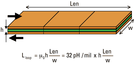
simple form, as illustrated in Figure 1.
|

FIGURE 1. Example of loop inductance of multiple power and ground planes or microstrip line over a return plane.
|
The
loop inductance for current going down one of the traces and back the
other one is just 32 pH/mil times the spacing between the traces and
times the ratio of the length to the width of the strips.
This
illustrates directly the three important knobs in physical design that
affect the loop inductance between conductors. The longer the loop, the
higher the loop inductance. The wider the traces, the more the current
can spread out, and the lower the loop inductance. In this special
geometry of spacing being small compared to the width, the relationship
between length and width scales linearly.
Finally,
this shows the third important design knob: the spacing between the
strips. The thinner the dielectric, the closer we bring the two opposed
moving currents and the more the rings of magnetic field lines from one
trace can cancel out the rings of field lines around the other trace.
The more overlap of opposite field lines, the less the number of field
lines and the lower the loop inductance.
The recipe
for low loop inductance is planes, on adjacent layers, with as thin a
dielectric as you can afford, to carry the PDN currents.
When
the length of the trace equals its width, the traces are shaped like a
square, and its loop inductance is just 32 pH/mil times the thickness.
For a 3-mil thick dielectric, this is 100 pH of loop inductance of the
square. We call this the sheet loop inductance. Every square cut from
this sheet will have a loop inductance of 100 pH.
The
loop inductance of a long, wide trace can be easily estimated if we
know the sheet loop inductance and how many squares it is long. If the
surface trace from a capacitor pad to a via is 120 mils long and 40
mils wide, which is 3 squares, its loop inductance, if the return plane
is 3 mils below, is 100 pH/square x 3 squares or 300 pH. If the plane
is 10 mils below, it will be 320 pH/square x 3 squares = 960 pH. This
simple approximation illustrates how significant the capacitor mounting
geometry is to the loop inductance of decoupling capacitors.
If
you want to minimize the inductance of capacitor surface traces, cut
the number of squares of surface trace from the pad to the via, and
decrease the dielectric spacing to the nearest plane. PCD&F
Next month: Looking at the origin of sheet inductance points to the important design knobs to optimize the PDN.
Dr. Eric Bogatin
is president of Bogatin Enterprises. This and other topics are covered
in the public classes Eric teaches. Check his web site for the
schedule: BeTheSignal.com. Send questions to This email address is being protected from spambots. You need JavaScript enabled to view it..


