Reducing the line width, just the right amount, keeps differential impedance constant.
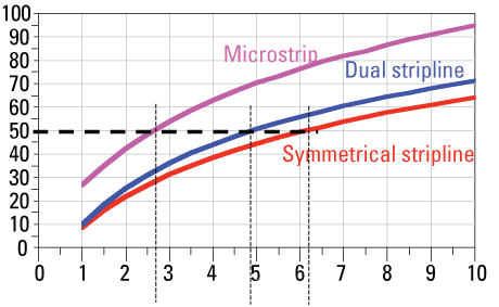
Every engineer responsible for stack up design has used a field solver at one time or another to determine how one or more physical features, like dielectric thickness, affects characteristic impedance. The field solver produces a curve (Figure 1) that helps to identify a nominal value to achieve the target impedance and immediately gives a measure of the parameter’s sensitivity to the impedance.
|

FIGURE 1. Characteristic impedance for different topologies each with 5 mil wide lines.
|
In this example, the dielectric thickness of each layer is varied while keeping the other parameters, such as line width (5 mil), metal thickness (0.7 mils) and dielectric constant (4.0) fixed. For these conditions, the design curve identifies the dielectric thickness of a 50 Ω transmission line in microstrip as 2.6 mils, each of the two layers between the planes in a symmetrical stripline as 6.2 mils, and each of the three layers in a dual stripline as 4.9 mils thick.
While these sorts of design curves are useful, they are not the most efficient way of exploring design space to reach the optimum set of design parameters.
Consider, for example, a set of layers where a different thickness may have a different dielectric constant, due to the type of glass weave and resin mix. The dielectric constant could vary from 3.8 to 4.5 in a typical glass-resin system. One approach to achieving a target impedance might be to start with a set of nominal values using the above sorts of curves, fix the dielectric thickness, find the combination of glass and resin to meet this thickness, and then, based on the dielectric constant, tweak the line width to bring the trace to 50 Ω.
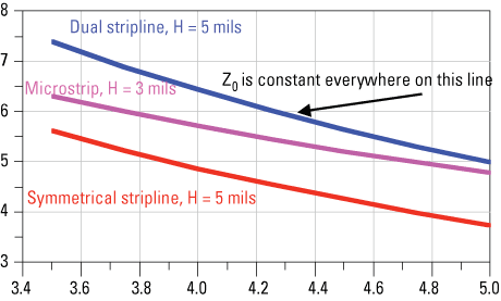
To explore this design space requires plotting a line of constant impedance (Figure 2). In this case, the dielectric thickness of each layer is fixed and the dielectric constant is varied while the line width is calculated to achieve 50 Ω. Everywhere on this line, the impedance of the interconnect is exactly 50 Ω. Meeting a target impedance value is really about riding this line. It defines the design space for a 50 Ω system.
|

FIGURE 2. Lines of constant impedance for different topologies, simulated with Agilent’s ADS.
|
As another example of the value of lines of constant impedance, consider the design of a symmetrical stripline differential pair. One approach might be to pick a set of parameters for a target differential impedance, like dielectric constant of 4.0, total dielectric thickness between the planes of 13 mils and metal thickness of 0.7 mils.
The last two parameters that influence the differential impedance of a pair are the line width and the edge-to-edge trace separation.
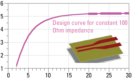
When the traces are far apart, a line width of about 5.2 mils would result in 100 Ω differential impedance. It is often the case that in routing the board, the lines might have to be brought closer together to snake through constrictions, such as connector fields, packages or other structure.
Of course, as the traces are brought closer together, the differential impedance will decrease.
However, if the line width were reduced just the right amount, the differential impedance can be kept constant. The relationship between the necessary line width for 100 Ω, as the edge-to-edge spacing changes, is shown in Figure 3.
|

FIGURE 3. Line of constant differential impedance in a symmetrical stripline, simulated with Agilent’s ADS.
|
As long as every pair on a layer is always “riding this line,†the differential impedance will be constant. The designer can then bring the traces closer together and reduce line width according to this curve to keep the impedance constant.
These types of lines of constant impedance can be generated manually or automatically with some field solvers. They are an instant map of design space and can increase your productivity by efficiently defining the stackup design for single ended and differential pairs. PCD&M
Dr. Eric Bogatin is president of Bogatin Enterprises. These and other topics are covered in the public classes Eric teaches. Check BeTheSignal.com for the schedule. Send questions to the Signal Doctor at This email address is being protected from spambots. You need JavaScript enabled to view it..


