The economic model for the optoelectronic interconnect favors high data rate transmission over moderate to long distances, limiting applications to high-end telecommunication systems.
Optoelectronic (OE) interconnect is an alternative to copper that can provide increased bandwidth and other advantages for special applications. For example, OE interconnect does not have the problem of “noise†that a copper interconnect can (a significant issue for high-speed communications). OE technology is also appealing for use in aircraft because it eliminates the weight of thousands of copper cables.
Several companies and laboratories are currently working on new waveguide technology and, therefore, OE substrate technology is continually changing. However, despite all the good research that has been accomplished, this technology has not moved forward. In North America, fiber cable is at the curb, but it has not entered the home, office or technical institutions. In Japan, fiber to the home is growing at a rapid pace.
Part of the reason for lack of movement of this technology is that continued improvements in (less-expensive) copper technology have kept pace with circuit bandwidth needs. Good design practice has also helped. However, as the thirst for faster signal processing continues and home electronics or distribution systems become the workhorse of every household, there may be applications that are willing to pay for the initial additional cost.
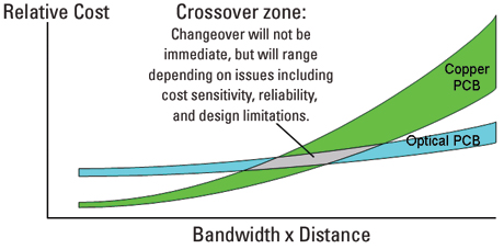
Optoelectronic substrates with embedded waveguides are still years from being in production, but they continue to be discussed and compared with traditional substrates. Many of the manufacturing dilemmas associated with optoelectronic substrates have to do with the cost and the reliability of the optical fiber polymer interface. OE substrates will not become prevalent until the cost-performance benefits are proven (Figure 1).
|

FIGURE 1. Copper vs. optoelectronic crossover zone.
|
This article discusses the current state of optoelectronic substrate technology and highlights some of the key issues surrounding its implementation, based on information from the 2007 iNEMI Roadmap.
Current State of the Art
The advent of increased data rates to support growing bandwidth requirements is certain to continue, and electrical transmission of signals will, presumably, soon run up against its limits.
Telecommunications systems appear to be the primary driver for optoelectronic interconnect technology. There are currently optical wide area and local area networks using fiber-based OE technology for infrastructure and hybrid fiber/organic substrates in the supporting backplanes. Today’s systems are generally operating at 10 Gbps, with 40 Gbps coming soon, and 100 Gbps already being discussed.
Signal conditioning technology has achieved bit rates on copper of 10 Gbps over high-performance and FR-4 boards. While this allows for electrical 10G line-speed on the backplane, it also adds cost and complexity. Furthermore, power dissipation is increasing, and edge density is limited. So optical interconnect solutions are still promising, but cost and technology reliability will determine the breakpoint.
For future generations of data and telecommunication, there is a growing demand for higher data rates and increasing performance. For PCBs in telecommunication systems, there is a growing need for better base materials and circuit board technologies for transmitting high-speed signals. It is clear that further advances in speed and bandwidth can only be achieved by taking advantage of new optical technologies for board-to-board and chip-to-chip interconnection on board.
Current Situation
Increased data rates to support growing bandwidth requirements are certain to continue. The timing of which applications will convert to optical technology remains unclear, but is not expected to happen within the 10-year period covered by the 2007 iNEMI Roadmap. The optoelectronic substrate technologies that will support the applications are also very unclear. Some experts believe the waveguide needs to be embedded or laminated between conventional base materials; other experts are developing waveguide technology external to the PCB.
Optical interconnect is expected to compete with copper interconnect technology for backplane and daughter card applications where data rates are 10-15 Gbps and higher. Both electrical and optical technologies suffer from signal attenuation and degradation problems that can be improved through circuit design and materials.
Optical Substrate Interconnect
Optical interconnects are being used on some boards today. Optoelectronics are currently used as the backplane interconnect if there is some architectural reason the signal needs to remain optical as it goes board to board, or if the system is distributed and a distance (typically > 1-10 meters at 5 > 5 Gbps) exists between connections.
Optical interconnections used in backplanes are currently fiber-based and exist as separate physical layers from the electrical backplane. The mechanical connection of the optical interconnect off the line card is done through a cut-out in the electrical back panel with an adapter placed in the cut-out. Optical jumpers or circuits are then plugged into the adapters to create the fiber connections in the backplane (the connections between cards). Issues with this type of interconnect include difficulties with cleaning and inspection, difficult fiber routing/handling and high cost.
Several different types of optical interfaces between OE components and circuit boards are being developed.
The optical path on the PCB or backplane. In current backplane technology, the optical path is generally provided through the use of optical fiber loops linking components to connectors or other optical or optoelectronics packages. The main issues with this approach are that it is impossible to perform any signal manipulation, and it is difficult to achieve high interconnect densities due to the limited bend radius of the optical fiber. Also, the difficulties in manufacturing and handling make this a costly and often low-yield approach. Because of the limitations of radius bending, this technology is limited to large boards (backplanes).
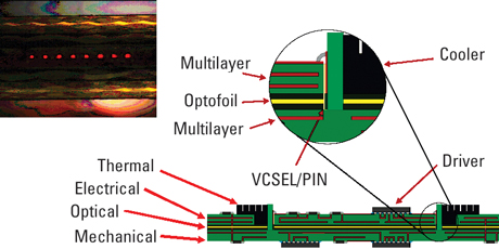
Optoelectronic module (component) connection to optical board (PCB) with integrated waveguides. Two coupling methods are being considered. The first is “free space†(without waveguide) interconnection using micro-lenses and special connectors; and the second is “direct butt coupling.†The direct butt coupling technique takes advantage of in- and out-coupling without any additional micro-optical elements, such as lenses and mirrors. The VCSEL-arrays/PIN-diode-arrays have to be positioned directly in front of the waveguide end. On the other hand, there are thermal and alignment problems, and the modules cannot be assembled using surface-mount technology processes (Figure 2).
|

FIGURE 2. Electrical optical circuit board (EOCB) using direct butt coupling.
|
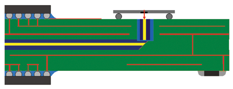
Guided wave, 90-degree beam deflection. Out-of-plane light deflection (Z-direction) can be accomplished using gratings (incoupling) or mirrors. A number of publications have demonstrated mirror fabrication by cutting the end of the waveguide with a dicing saw, wet chemical etch or laser to create a 45° facet. The facet can be metallized to improve the reflection properties of the mirror. Mirrors have the advantage of being wavelength independent, but can cause high losses due to surface roughness of the mirror surface. Aligning the mirror to the waveguide and active device poses significant problems, and will have to meet similar tolerances as required for the transmitters and receivers (Figure 3).
|

FIGURE 3. EOCB using 90-degree beam deflection and waveguide pin.
|
Materials and Processes
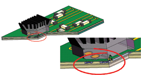
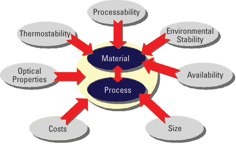
Cost of the materials and the associated processes need to be considered when developing materials to meet optoelectronic performance specifications. There are a number of inorganic materials that can be used for embedded optical interconnects, including Si/SiO2 silica and glass sheets. Of these, only glass sheets have been applied to embedded waveguide technology for PCBs (Figure 4).
|

FIGURE 4. The glass layer concept.
|
SiO2 and silica materials are used in device applications and are processed directly on silicon wafers. Waveguides are formed through a combination of lithographic printing, etching (wet chemical or laser) or ion implantation.
The material of choice, whether it is inorganic or organic in composition, needs to be compatible with the board manufacturing environment and equipment. The material will be exposed to various chemicals and temperatures, handled most of the time outside a cleanroom environment and cannot be sealed hermetically. It also should be compatible with standard processing (lamination, etching, drilling, soldering, etc.) techniques.
Any new material introduced as a waveguide solution for PWB interconnects needs to undergo extensive reliability testing, including failure analysis. Similar requirements extend to the electro-optic hybrid laminates and assembled boards (Figure 5).
|

FIGURE 5. Optimization of waveguide material and PCB technology.
|
Some of the techniques used for polymer waveguide structuring include hot embossing, photolithography and laser writing. In particular, for medium-sized boards and if large amounts of waveguide foils for mass-production are desired, hot embossing seems to be the most promising technology. However, for the up to 1 meter waveguides needed in backplanes, lithographic or laser writing techniques appear to be the most appropriate. Recently, a working EOCB (electrical-optical circuit board) with hot embossed planar polymer waveguides was demonstrated.
Optical PCB Manufacturing
The integration of optical components into the world of PWB manufacturing will significantly impact the PCB operating environment. Most PCB manufacturing facilities have a limited or “selective†focus on the operating environment. The imaging areas of most shops contain a “Class 10K†cleanroom for the expose operation. Some have improved areas for optical testers and laser drilling.
The PCB manufacturing shop will need to change significantly to integrate optoelectronics. This same degree of change will also apply to the PCB component assembly operations. Waveguide processing will require very clean manufacturing environments, and optical component assembly will require precision micron placement techniques. Both of these will require improved temperature, humidity and cleanliness requirements. Once the boards are assembled, the cleanliness of the product needs to be ensured by active means such as air filters or passive protections such as connector doors and dust seals.
Emerging Technologies
Several emerging technologies may impact optical interconnects and OE components. These include photonic crystals or optical band gap materials, complex gratings and new material systems. The list is growing continually as more R&D effort is put into optoelectronics. It is impossible to predict which emerging technologies will be pervasive in the future.
Table 1 [PDF format] summarizes some of the promising technologies being developed that might “disrupt†our current vision into the future and provide a solution to the challenges previously discussed.
Conclusions, Gaps and Needs
OE technologies are used in mainstream, high data rate applications when they offer a lower cost than the alternative of using copper (or sometimes wireless) methods. Since optical technologies are newer than copper methods, their cost is falling faster. As the cost of optical transmission drops, the distance at which optical methods are more economic becomes shorter, and today, optical methods are sometimes more economic for high data rates over distances of 10-100 meters. In the future, optical methods are likely to be used at even shorter distances as demand for high data rate transmission continues to grow. There is increasing interest in optical chip-to-chip connection on the system board to overcome bandwidth bottlenecks between the CPU (clock speeds up to 10 GHz) and the main memory or I/O bus (running at hundreds of megahertz).
The following enablers are needed to make optoelectronics a more mainstream technology:
Laminated and embedded waveguide interconnect development for high-speed optical backplane and chip-to-chip applications are needed. In addition to the need for the optical interconnect, there will also be a requirement for transmitter (VCSEL) to waveguide to receiver coupling and small radius 90° bends.
Improved VCSELs, for 1310 and 1550 nm transmission are needed, with sufficient reliability for thousands to be used in systems that have less than 15-year lifetimes.
Outsourcing of manufacturing by OEMs to CEM and EMS companies will lead to wider dissemination of closely held package, assembly process and test knowledge.
A major impediment to acceptance of lower cost “datacom†components by network service providers is the requirement for rigorous reliability and testing to “telecom†standards, such as Telcordia GR1221. There is a real need for “lite†standards, suitable for products with 10-15 years’ field life. Examples include use of epoxy adhesives inside OE packages and non-hermetic (but acceptably impermeable) materials, such as Liquid Crystal Polymer (LCP), which have been used in electronic packages to MIL spec for years.
Measures of the current and future cost of OE interconnect vs. copper as a function of application, data rate and distance are badly needed. The cost to provide data rate drives OE. We were unable to find clear measures of the cost of OE vs. copper except at higher levels, such as long-haul telecom systems. Cost details at level 2 would be helpful to determine the economic gaps that OE technology might address and would provide a cost-performance basis for the technology roadmap.
Emerging technologies such as holey fibers, photonic band gap materials and solutions hold promise of providing alternative methods of transmitting and controlling optical signals in ways that may be commercially important in the future. Optical electronics technologies are emerging continually; we need to watch for important developments and keep an open mind. PCD&M
Jack Fisher (This email address is being protected from spambots. You need JavaScript enabled to view it.) is a consultant (Interconnect Technology Analysis) and chair of the organic interconnect chapter of the 2007 iNEMI Roadmap. For additional information about the iNEMI Roadmap, go to inemi.org/cms/roadmapping/2007_iNEMI_Roadmap.html.


