To accommodate faster signal rise and fall, designers need to apply good placement and routing techniques.
Many years ago, PCB designers did not really need to understand what was happening electronically on the boards they designed. They basically used the placement rules that were given to them and then just connected the dots and moved on to the next board. But changes in the electronics industry have caused the speeds of parts and, thereby, the speeds of the designs to increase dramatically. The changes show no signs of slowing down. The more complex the parts and the faster signals rise and fall, the more the board needs to be “controlled†with good placement and routing techniques. Connecting the dots has not been an option for many years.
Designers need to understand some basic electronics in order to make good decisions when designing boards. If one understands how certain issues affect other issues in the board or trace structure, then one will design a better board the first time. And isn’t that the goal of all designs – to be done correctly, without changes? There are many complex issues involved in the definition of each of the items that will be discussed, but this article will attempt to give a basic definition to a few electronic terms and explain why each is important to the designer and the designs they create.
Current is the flow of electrons past a certain point. If there is no connection at the far end of the wire, there is no place for the last electron to go, and current does not flow. When there is a connection and electrons do move, they flow in a loop, and the amount of current must be constant at every point throughout that loop. For this reason, the signals on the board must return to their source, and designers must plan for that return current by designing a path for it as well.
Current also helps determine the needed trace width on a board and also temperature rise. If there are too many electrons fighting to go through a trace that is too small, some of the energy is converted to heat energy, raising the temperature of the trace and the area around it. Keeping the boards at a working temperature that is as close as possible to ambient is a very good thing for the life of the product. Designers should pay attention to the amount of current in the signals on the board and adjust the trace width accordingly.
When current flows through conductors, there is inductance. Inductance is like the anti-current in that it is the opposition to any change in the flow of current. This means if there is no current on the trace, inductance acts to briefly prevent it by building up magnetic fields first, before the energy can flow. Conversely, if there is current on the trace, inductance slows the dissipation of it by using up the energy in the magnetic fields before the current is completely dispelled.
Since inductance always exists on a board, the designer must know how to control it. The magnetic fields are most problematic when they are changing. Signals that change often or change rapidly cause more interference to other signals. If the magnetic fields from one signal cut through a neighboring trace, they can induce a voltage in that trace when none should be there, causing problems on that signal. Extra spacing between traces would help in this instance.
The inductive loop area should always be kept as small as possible. In order to keep the magnetic fields to a minimum, planes should be placed as close as possible to every signal layer. This reduces the loop area of the return current and allows the magnetic fields to partially cancel each other, reducing interference.
Another way to control inductance is shorter traces because they create a smaller loop area and possibly keep the signal from reaching its maximum interference potential. Inductance also decreases very slightly if the trace is wider or thicker, but the percentage of decrease is so small it is insignificant (1 to 2%).
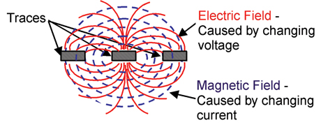
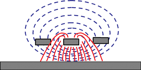
Voltage is the pressure that causes the current to flow. As it does, it forms electric fields. When the electric fields are changing rapidly, there is more high-frequency energy available to cause interference with other signals just as the magnetic fields do. These fields are always present when energy is transmitted, whether in the air or on a transmission line, so the best we can do is control and avoid them. Nearby planes will help here by capacitively coupling the electric fields to the planes as seen in Figures 1 and 2. Also, the voltage helps determine the needed spacing between traces. Extra spacing means less ability to interfere.
|

FIGURE 1. Electric and magnetic fields without planes.
|
|

FIGURE 2. Electric and magnetic fields with planes.
|
The opposition to the change in voltage in a circuit is capacitance. It is formed when two conductive surfaces of different voltages are separated by an insulating material. A charge will build up between the “plates†until it is equalized on both sides. That charge is the inertia to any more voltage change. Eventually, when the volt does change, current will flow through the capacitor.
Basically, if the planes on a board are charged but beginning to drain because of parts turning on, bulk capacitors try to keep those planes fully charged by “contributing†their own stored energy. If the planes are uncharged, they fill up the bulk capacitor first. Then the current will flow through the capacitor to charge the planes.
PCB traces form capacitance with all adjacent conductive surfaces whether they are intended to or not. The strongest capacitive region is between the trace and its return plane. It increases when traces or planes are made larger or wider, and it also increases when traces or planes are brought closer together. This is very good for high-frequency decoupling of high-speed circuits.
Resistance is another form of opposition to the flow of electrons. It acts like a crimp in a hose where the size of the crimp is the value of the resistor in a circuit. To maintain the same flow of electrons with a crimp, you would have to increase voltage. An example of increased resistance in a board is the skin effect that is formed when the magnetic fields associated with very high-frequency signals push the majority of the electrons to the outer “skin†region of the trace. The full cross-sectional area of the trace is not being used. Therefore, the trace has higher resistance and impedance. Some side affects of increased resistance are more high-frequency energy (dv/dt) and heat.
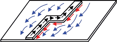
A transmission line is simply a signal trace, and its return path as shown in Figure 3. As an electronic wave (signal) travels on a trace, it also must return an equal amount of current to its source. Remember that current must flow in a loop. It does this by capacitively coupling that current to the nearest plane, which should be only one layer away for the lowest possible impedance path. In a properly stacked digital board, all the traces are well-controlled transmission lines because planes have been placed right next to every signal layer on which the return current can travel.
|

FIGURE 3. Transmission line.
|
The return current on the plane will follow the path of the original signal exactly, instead of spreading out on the plane like the DC return will as noted in Figure 4. This is because at signal speeds above a few hundred kilohertz, the return current will follow the path of least impedance, which is the exact same path as the signal.
|

FIGURE 4. Return current.
|
The most common causes of crosstalk and EMI are problems between the trace and its return path. If there is an accidental separation of signal and its return path, signals will lose their tight coupling to one another, causing increased impedance and increased coupling to other signals. Designers must be careful not to build obstructions into the return path like via dams, splits in planes and antipads. The return path must be planned just as the signal path is planned.
The combination of the resistance, inductance and capacitance per unit of transmission line is what we call impedance. At low frequencies, resistance is the major factor in impedance, but at frequencies above a few kilohertz, inductance and capacitance work together with resistance to create a constant opposition to the change in voltage or current in a circuit, and thereby, opposition to the flow of a signal (energy) in a circuit. The value of that constant number is the number we use as the given impedance of a trace. The goal of a controlled impedance board is to have a constant impedance on traces and layers or at least to control it within allowable limits.
Many factors affect the impedance on the board. If capacitance increases, impedance is lowered. If inductance increases, impedance is raised. Designers can control impedance by control of trace width, trace proximity to plane, trace proximity to other traces, controlling stubs and reflections.
Crosstalk is the transfer of energy from an active source to a victim circuit. It is caused by such factors as stray magnetic and electric fields interfering with a quiet signal; poor impedance control; false triggering; and placing victims and sources too close together. The faster the signals are on a board, the higher the harmonics that are available to cause crosstalk problems.
Crosstalk is localized EMI (electromagnetic interference) in the near field (within1/6 wavelength to a source of energy) and must be controlled in much the same way as EMI is controlled on a board. Some of those ways are to allow as much spacing between signals as possible, place a plane layer for every signal layer in the stack-up, minimize parallelism of traces, control reflections and handle I/O signals with extreme care to minimize crosstalk entering or exiting or forming on the board.
Conclusion
Board issues are changing as quickly as the parts we put on them. The issues discussed here are only a very few of the ones that affect board layout. It is up to designers to understand all the factors involved and how to control them in order to design high-quality boards. PCD&M
Susy Webb is a senior PCB designer. She can be reached at This email address is being protected from spambots. You need JavaScript enabled to view it..


