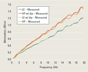
Smooth copper minimizes signal attenuation at high frequencies but it can negatively impact product reliability by reducing innerlayer bond strength.
One of the great things about the electronics industry is that there is constant and sometimes rapid change across many aspects of the business. The changes I am referring to generally fall into two categories: cost driven changes and performance driven changes. Both of these drivers can manifest themselves in many different ways. Though PCBs are basically the same structures they have been since their early days, i.e. traces and holes that interconnect numerous components and connectors that are mounted to them, the methods used to fabricate PCBs, the materials used and performance requirements that must be met have changed dramatically over the last decade.
As our industry continues to implement changes in the name of cost reduction or performance requirements, little surprises can pop up (read, problems) that need to be understood and addressed. In this article I’d like to discuss one of these little surprises that has a number of OEMs working on understanding its effect, how to measure it and how to control it. The surprise I am referring to is the effect that an oxide or oxide alternative has on the electrical signal performance in a given system or subsystem. Until recently, very few companies considered oxide or oxide alternative treatment and its effect on signal attenuation into their overall system performance budget. I also want to raise overall awareness of a few of the other the lesser-known variables that can occur in the real world that can cause system performance variation.
Many of you know that there are a number of influences that can affect an electrical signal in a PCB. As signal frequencies continue to increase, and companies continue to push FR-4 materials performance levels as a cost control effort, it is even more important to understand, or at least be aware of, the various factors that can play a role in causing system performance variation.
The single most important influence on signal performance is the laminate dielectric material and its various components used to make up the laminate composite. These variables include the resin type, resin content, glass weight, glass style, number of glass plies, copper weight and copper type. Most of these laminate component influences are fairly well understood, and the various resin systems and glass fabrics have proven electrical performance levels that can easily be measured using a number of different methods. Many of the larger OEMs have developed specific test protocols for measuring electrical signal performance and use these test methods to help identify “preferred” laminate material types and PCB construction criteria for various levels of technology. IPC also provides measurement method protocols as well as sponsoring committees working on standardization of protocols and test vehicles.
Though this all sounds fairly straightforward, there are many nuances and variables that many folks, especially within design groups, may not take into account. For instance, did you know that many laminate materials, both c-stage and b-stage, can be purchased with varying resin contents? Resin content has a direct and considerable effect on signal attenuation, and if a fabricator doesn’t control it, or if the OEM doesn’t specify resin content, an additional variable has been added to the long list of items that can affect system performance. Another lesser-known variable that can occur in a given laminate family is the fact that various C-stage cores in the .004 to .008-thickness range can be purchased with one or two plies of glass fabric laminated into them. Similar to resin content, this is a construction variable that needs to be controlled in order to minimize system performance variation. Things start to get even more complicated when you factor in the seemingly endless variety of laminate resin types available on the market today. It seems that there is a “specialty” laminate for all needs these days.
The copper foil type used in a given lay-up can also influence signal attenuation at higher frequencies, albeit at a much lower weighted influence than the glass and resin. Variations in the type of copper used in a specific PCB design that is sourced across multiple PCB suppliers may vary quite a bit and can ultimately result in potential, though somewhat marginal, system performance variations. Copper foils come in a variety of thicknesses, typically ranging from 1?8 oz. to 3 oz. in conjunction with varying surface treatments including double treat, reverse treat, shiny foil and R/A. Additionally, some of these foils can also be purchased with varying profile heights of the dendrites, i.e. low profile. Dendrites are the bumpy little protrusions on one side of the foil that are formed during its manufacture. Add to this the availability of different copper grain structures such as standard vs. HTE (high tensile elongation) foil.
As you can see, with just the three components that go into a laminated composite (resin, glass and copper), and a multitude of variations within each of the three categories, there are literally thousands of potential combinations. Detailed material specifications, both at the PCB fabricator and from the OEM/CEM, are key to ensuring consistent system performance. In today’s world where system signal speeds are approaching the 3, 5 and even 7 GHz range, materials control becomes even more important.
Recently, a number of OEMs have identified yet another variable that has a significant effect on signal attenuation. It is especially important in some of the larger form factors such as routers, data storage, high end computing and servers where signal trace length tends to be significantly longer vs. a small handheld device like a mobile phone or MP3 player. The new factor people are taking a closer look at is the variation in innerlayer copper surface roughness that is the result of the various oxides and oxide alternatives that are used to impart a rough surface onto the innerlayer copper features. This rough surface enhances the bond between the b-stage resin and the innerlayer copper in a multi-layer PCB, and also acts as a barrier layer to prevent the corrosive effects some resin systems have on copper.
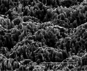
Over the last decade or so there has been a continuous shift away from the traditional oxides and reduced oxides to what is generally referred to as oxide alternatives or OAs. OAs are essentially highly modified etchants that impart a rough surface to the copper via a complex set of chemical reactions and results in a uniform, thin micro-roughened, organo-metallic surface. An example of a copper surface that has been OA treated can be seen in Figure 1. For reference, the example in Figure 1 is a reverse treat HTE foil treated with a commercially available OA process. Note the “English muffin” appearance of the copper surface.
|

FIGURE 1. Reverse treat HTE foil treated with a commercially available oxide alternative process A.
|
Historically, “the rougher the better” was the general feeling as it related to the resultant OA surface. This position was based on the premise that if the copper is rough the mechanical bond between the b-stage resin and the copper surface should be enhanced. This is essentially true, but in today’s world where signal frequencies continue to increase this mindset needs to be recalibrated. Yes, rough copper is good from a bonding perspective but roughness has a definite negative effect as it relates to signal attenuation.
There is a fairly well known phenomenon called “skin effect” that comes into play when signal frequencies increase. Numerous papers have been written on the topic going all the way back to 19481. Figure 2 shows the formula for calculating skin effect.
|

FIGURE 2. The formula for calculating skin effects.
|
At lower frequencies electrons tend to flow through the entire cross section of a conductor. As the frequency increases, the electrons tend to move toward the outer surfaces of the conductor and may ultimately flow only on the outer surfaces, or skin, of the conductor if the frequency is high enough. This is where innerlayer copper surface roughness comes into play. If the surface is roughened using typical OA chemistries, you are essentially increasing the distance an electrical signal needs to travel when running at higher frequency levels. This in itself is not an issue if all the PCBs of a given design used in a system utilize the same materials and OA surface treatment. Unfortunately, in the real world where PCBs may be sourced from numerous fabricators around the planet, the variations between fabricator OA processes can, and indeed does, result in unacceptable system performance variation.
|

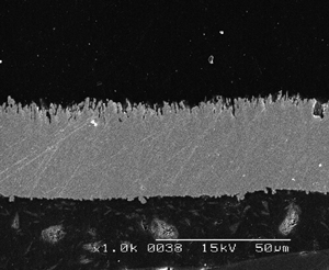
FIGURE 3. Cross-sectional photomicrographs of commercially available oxide alternative process A.
|
|

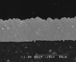
FIGURE 4. Cross-sectional photomicrographs of commercially available oxide alternative process B.
|
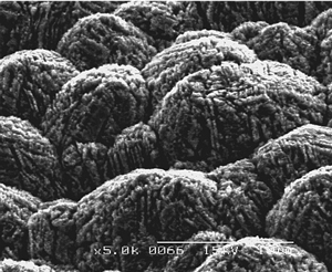
Figure 3 and Figure 4 depict cross-sectional photomicrographs of the disparate effects two different commercially available OAs have on the surface of the innerlayer copper. Figure 1 and Figure 5 are oblique-angle SEM photos of the same foils with the same two different OA treatments. The samples were produced using the same equipment with the same HTE reverse treat copper foil so the only variable in the two samples was the chemistry used to process the innerlayers. Now imagine these samples happen to represent the process output of two different PCB fabricators. Do you think it would affect system performance due to attenuation variations? Depending on the frequency your particular system operates at, the answer is yes, it could. This exact scenario has recently been proven to be the root cause behind performance issues identified at more than one large OEM.
|

FIGURE 5. Oblique angle SEM photos of oxide alterative B.
|
The chart depicted in Figure 6 illustrates the delta in electrical performance between the samples shown in Figures 1, 3, 4 and 6. As you can see, as frequency increases, the electrical performance of the two OAs begins to diverge as measured by SPP2. As an example, at about 4 GHz the signal attenuation difference is approximately 2 dB/cm when comparing one OA vs. the other. As mentioned earlier, depending on trace lengths in a given PCB design, this delta in signal attenuation can potentially affect system performance.
|

FIGURE 6. Delta in electrical performance between the samples shown in Figures 1, 3, 4 and 6.
|
So where does this leave us? Assuming we continue to see systems running at higher and higher frequencies, it’s imperative designers and engineers understand all the variables that can affect signal attenuation. In this author’s humble opinion, there is room for improvement in the materials control and specifications area.
Based on the aforementioned information one could jump to the conclusion that high frequency systems should convert to smooth copper, right? As with everything else in life, it’s not quite that simple. There will need to be intermediate steps between what is available in the OA market right now vs. where we would like to be.
Smooth copper on the innerlayers certainly would be advantageous in minimizing signal attenuation at high frequencies but product reliability, i.e. thermo-mechanical robustness, would most likely suffer since the bond between b-stage resin and smooth copper is very weak. Most PCB chemical supply companies provide a variety of OA products that impart varying degrees of surface topography, and an important first step may be to baseline what processes are being used on your PCBs and what potential options are available. As you can see in the photomicrographs in this article, even today there are OA options that provide incremental electrical performance advantages yet still maintain the overall thermo-mechanical reliability of the PCB.
Another area of consideration is the fact that PCB fabricators typically do not measure the roughness of innerlayer copper, nor do they typically have the metrology available to do so.
Ultimately, for those of you who deem variation in innerlayer copper roughness as a potential performance issue there is a lot of work ahead. Since this issue has only recently been identified as the causal effect in system performance variation there is little knowledge to draw upon within the industry. Metrology options, copper roughness thresholds and thermo-mechanical reliability will most likely be initial focal points so that a firm understanding of the various OA processes outputs, i.e. relative roughness, and how that relative roughness affects a given PCB design, can be fully understood. PCD&M
Bruce Lee is the Specifications manager of OEM and Assembly Applications for MacDemid Inc. He can be reached at This email address is being protected from spambots. You need JavaScript enabled to view it..
REFERENCES
1. Effect of Surface Roughness on Eddy Current Losses at Microwave Frequencies – Morgan 1948
2. Short Pulse Propagation alphaworks.ibm.com/tech/gammazandcz2d


