A high-speed signal crossing splits of a reference plane can experience undesirable electrical impact.
Ed. – This column was published in two parts in the February and April issues. Both parts are included here.
Routing high-speed signals over slots of the nearby reference plane can cause undesirable effects such as impedance discontinuities (destructive reflection), EMI noise1 and crosstalk. The reference plane may be a ground or a power layer.
One effective approach for gaining insight regarding the effects of plane split boundaries is to consider the nature of current flow. When a high-speed current travels along a PCB trace, an equal and opposite return current2 flows in the reference plane underneath that signal track. This current returns in a manner to diminish the total impedance3.
At low frequencies this translates to minimizing resistance by spreading over every possible path. At high frequencies the return current crowds under the signal (on reference plane) to minimize inductance. An interesting way to visualize the current pattern on a reference plane is to define/model the geometry consisting of trace(s) and planes using FastHenry, a free 3D field solver. Then generate a set of current distribution files and plot them by applying Matlab commands4.
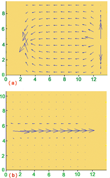
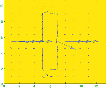
Although this approach has certain limitations it can provide useful understanding regarding the behavior of the return current. Hence, this technique was applied to simulate a trace with a solid reference plane and a trace-crossing plane split. For each case the trace length, width and thickness were set at 4 inches, 7 mils and 0.72 mils, respectively. The trace to plane height was 5 mils and the width of plane slot equaled 10 mils. The results for low frequency (f = 1.0 Hz) and high frequency (f = 100 MHz) excitations are presented by Figure 1 and Figure 2.
The results of Figure 1 verify that for low frequencies the return current (traveling from source to sink points) spreads4 across the plane, whereas at high frequencies the current is focused beneath the signal trace.
|

FIGURE 1. Return current distribution on a solid reference plane at (a) low frequency and (b) high frequency.
|
|

FIGURE 2. Return current distribution for a high frequency signal crossing a split plane.
|
Figure 2 demonstrates the high frequency current distribution for a split in the reference plane. FastHenry, in conjunction with Matlab, were again applied to model the geometry, compute the current distribution and plot the outcome. The outcome illustrates that the slot interrupts the path of the return current forcing it to find a way around the discontinuity.
One unusual feature of this visualization method is that sometimes current vectors4 point into empty space (plane gap). This happens because current vectors do not precisely exhibit the current flow at a given point.
Slot of any width can cause a current diversion, which in turn increases the loop area and inductance5 of the signal path. This leads to added crosstalk, and EMI and rise-time degradation. It is desirable to avoid slots in planes for high-speed PCBs, but they can occur in certain situations.
Sometimes ground layer splits happen because a board designer runs out of space on a regular routing layer and places tracks on the ground plane5 by cutting a slot in the plane layer for routing traces. Ground slots can also occur due to improper5 connector layout. A power plane with splits results when multiple powers are incorporated on the same plane layer. Power islands6 are among the most evident split-plane circumstances. The island’s boundary, or moat, defines a total break6 in the copper plane resulting in an isolated area. This approach is often applied to create unique power regions that connect either to the same voltage via a PI filter (composed of shunt capacitors and ferrite/inductor) or to a voltage different from the rest of the plane.
If a high-speed net is routed perpendicularly over moats, the signal trace will experience added inductance, degraded rise-time, crosstalk and EMI. Hence, an excellent rule is to avoid the routing of high-speed nets over plane splits; however, the complexity of modern high-speed PCBs may impose violations of this guideline.
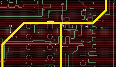
Figure 3 displays a section of a multilayer board produced using the Cadence Allegro PCB Design Software. The PCB was examined utilizing Allegro Free Physical Viewer program by turning on the desired signal layer and its reference power plane with other layers turned off. The plane layer has a gap G due to boundaries of multiple power islands. Here the gap width is 20 mils. There are several traces (T1, T2, T3 and T4) of the signal layer routed over splits of reference plane. C1 and C2 outline two stitching capacitors (small valued caps with values ? 1 uF) to bridge the plane splits. The adverse effects of plane slots on high-speed signals crossing them can be minimized by implementing another plane tightly coupled7 via bypass and interplane capacitance. Such capacitance furnishes an AC path for the signal’s return current and supports the switching edges. The slots should not occur at the same location in both or all planes.
|

FIGURE 3. PCB signal traces routed over voids of the nearest reference power plane.
|
Stitching capacitors8, when properly placed, can reduce current loop area, lower impedance discontinuity, and minimize adverse effects on signal quality and EMI due to the crossing of splits. The ends of stitching capacitors need to be connected to each plane detached by the split.
The implementation method and location of capacitors play an important role in determining their effectiveness. In one study9, applying a 600 MHz clock with 300ps rise/fall times, a 0.1uF stitching capacitor was placed at one side of a signal bus (crossing plane splits) at distances of 1, 0.5 and 0.1 inches and directly adjacent to the edge-line. The signal waveform and overall radiation for these configurations were ascertained via simulation. It revealed that capacitors should be placed near (within 100 mils) the edge line. The capacitor became ineffective9 when located more than half an inch away.
The proper analysis and design of current return path for high-speed PCBs can be critical for achieving optimum system performance. The return current loop is often unclear from design’s schematic drawing10, which mainly illustrates electrical connections of circuit components or signal flow. The return current is influenced by board layout, stackup, via transitions11, connectors and voids/splits in reference ground/power layers. For instance, the stackup should furnish a plane layer close to every signal layer. Incorporating adjacent power and ground planes can also prove beneficial. Placing a decoupling capacitor11 near a via can aid completing the return path and diminishing energy loss. The connectors need to provide sufficient number of return path connections. The same signal trace reference should be utilized on both sides of a connector11. Routing a high-speed signal across a plane gap should be avoided whenever possible.
A plane split can interrupt the return current, and adversely affect EMI, crosstalk, signal rise/fall times, inductance or impedance. TDR can be applied for examining impedance changes in single-ended and differential traces due to crossing of moats. A set of TDR measurements was conducted employing an Agilent 86100A Infiniium DCA mainframe with an Agilent 54754A differential TDR module.
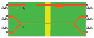
Two Agilent demo boards were utilized12. Each included a single-ended microstrip and an edge-coupled differential pair. The single-ended traces had variable width (hence links of various impedance) along their length. Figure 4 depicts the demo board traces with SMA connectors at each end.
|

FIGURE 4. TDR test board having single-ended (a) and differential lines (b).
|
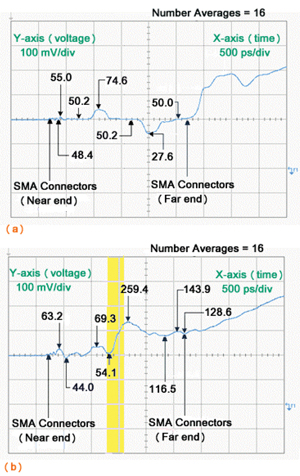
One of the test boards had a solid reference ground layer while the second board had a ground plane with a 1-inch wide gap. The yellow region highlights the plane gap’s area.
Prior to DUT measurements, a sufficient warm up period was allowed and calibration and normalization were performed13 to produce accurate TDR data.
Figures 5a and 5b reveal that the peak impedance of the single-ended line increased due to crossing a void. Regardless of a moat’s width, the impedance increases in the region associated with the signal crossing the void because of a larger return path loop (causing the inductance to increase) and a decrease in the capacitance6.
|

FIGURE 5. TDR response for microstrip track of the test board with a solid reference plane (a) and a split plane (b).
|
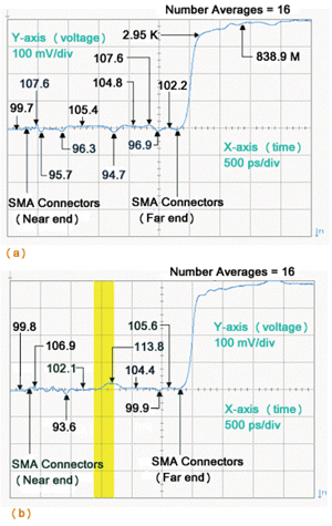
TDR measurement results for the differential pair are presented by Figures 6a and 6b. They illustrate that differential impedance has increased due to the traversing of the gap.
|

FIGURE 6. TDR signature for differential lines of the test board with a solid reference plane (a) and a split plane (b).
|
The highlighted region on Figure 6b displays the extent of the plane gap. TDR results indicate that crossing the plane slot has less effect on the differential pair vs. single-ended because each signal in the pair is affected identically6 due to traversing the plane void.
Additionally, a gap in the return path causes a significant increase in crosstalk for single-ended traces due to high mutual inductance. Hence, whenever traversing a gap is unavoidable, it is preferable to consider a differential pair14 (as compared to single-ended) that can cause lesser distortion of the signal, although some increase in differential impedance and little common-mode voltage.
The TDR test board had a large gap (1 inch) to simplify measurement of effects. The splits in high-speed PCBs are usually much narrower. A common value for power-plane moat is ~ 10 mils.
The return path for a high-speed signal is not limited to PCB structures but usually extends inside IC packages15 of the driver and receiver devices. Subsequently, the package bond wires, traces, power/ground planes16 and solder balls contribute to the signal loop area. The IC pin out may provide useful information regarding package structure. For instance, a signal net encircled by ground pins is probably ground referenced15 on the package and the same referencing is preferred on a PCB towards optimizing the return path.
A topology was defined using Signrity’s Speed 2000 to investigate signal degradation caused by a high-speed signal traversing a plane split16 inside an IC package. The topology included three microstrip traces as illustrated by Figure 7. Two cases were simulated: 1) the reference plane was a solid ground, and 2) the reference plane contained a slot. The void area is highlighted yellow.
|

FIGURE 7. Three coupled IC package traces traversing a plane gap.
|
Each trace had a driver consisting of a current source in parallel with a 50-Ohm resistor. The current source outputted a pulse with 100ps rise/fall times, 300 ps duration and 50-mA amplitude. The load end of each trace connected to a 60-Ohm resistor.
The package trace dimensions included 2-inch length, 2.8-mil width and 1.2-mil thickness. The edge-to-edge spacing of adjacent tracks equaled 5.12 mils. The dielectric substrate thickness equaled 3.94 mils with a dielectric constant of 4. Multiple/coupled traces were defined since coupling effects happen frequently in IC packages.
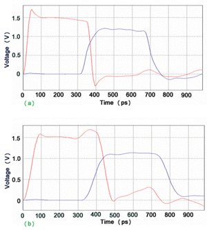
The simulation results for an active net are depicted by Figure 8. A comparison of Figure 8a and 8b reveals changes in both the driver (in red) and load (blue) waveforms because of impedance discontinuities created by plane slot. The signal rise time has been slowed/degraded due to traversing of plane gap.
|

FIGURE 8. Driver and receiver waveforms for a signal with a solid reference plane (a) and a split reference plane (b).
|
In conclusion, crossing a reference plane void can cause adverse effects such as rise time degradations, impedance discontinuities, EMI noise and crosstalk. These adverse effects may be diminished by proper use of stitching capacitors. The required number of stitching caps is directly proportional to the number of signals crossing plane gaps. The negative impacts of split reference planes on EMI and signal integrity can be further minimized by applying an effective termination17 scheme. For an inner layer, sandwiched between a uniform ground layer and a plane with multiple power islands, a logical strategy is to design the stackup with the inner signal layer placed close to the solid ground and far from the split power plane. PCD&M
Dr. Abe (Abbas) Riazi is a senior staff electronic design scientist with ServerWorks (a Broadcom Company) in Santa Clara, CA. He can be reached at
This email address is being protected from spambots. You need JavaScript enabled to view it..
ACKNOWLEDGEMENTS
Special thanks to Peter Arnold, Richard Kuo, Clement Yuen and Manvender Raghav for reviewing this article and furnishing valuable feedback. My gratitude to Mahrokh Esfandiary and Dean Gonzales for helpful discussions. Special thanks to John Dorighi of Agilent Technologies for furnishing the TDR test board with split plane.
REFERENCES
1. Doug Brooks, “Slots in Planes,”
Printed Circuit Design, March 1999, PP. 36-37.
2. Howard Johnson, “Visible Return Current,” online newsletter, Vol. 8, Issue 08, 2005.
3. Brain Young, “Digital Signal Integrity Modeling and Simulation with Interconnects and Packages,” Prentice Hall, 2000, P. 413.
4. M. Kamon, C. Smithhisler, J. White, “FastHenry User’s Guide,” Sept. 26, 1996, PP. 32-38.
5. Howard Johnson and Martin Graham, “ High-Speed Digital Design; A Handbook of Black Magic,” Prentice Hall 1993, PP. 194-197.
6. Stephen C. Thierauf, “High-Speed Circuit Board Signal Integrity,” Artech House, Inc., 2004, PP. 95-98.
7. Lee Ritchey, “Examining Rules of Thumb,”
Printed Circuit Design, Jan. 2000, PP. 36-38.
8. “High-Speed USB Platform Design Guidelines, Rev. 1.0” Intel, 2001, P. 8.
9. Juan Chen, Weimin Shi, Adam J. Norman, Ponniah Ilavarasan, “Electrical Impact of High-Speed Bus Crossing Plane Split,” IEEE International Symposium on Electromagnetic Compatibility, 2002, PP. 861-865.
10. Bruce Archambeault, “EMC Effects from the Hidden Schematic”,
Printed Circuit Design and Manufacture, January 2007, P. 18.
11. Scott McMorrow, “Handling Signal Return Current”,
Printed Circuit Design, September 2002, PP. 12-16.
12. “User’s Guide Agilent 54753A and 54754A TDR Plug-in Modules”, Third edition, Agilent Technologies, 2000, PP. 7-19 to 7-23. PP. 8-10 to 8-13.
13. Abe Riazi, “TDR For Differential Pair Characterization”,
Printed Circuit Design and Manufacture, September 2005, PP. 16-18.
14. Eric Bogatin, “Differential impedance finally made simple”, Bogatin Enterprises 2000.
15. Kim Flint, “Seeing the Big Picture” July 2005.
16. “Trace Over Split Plane”, Benchmark Test Report, Sigrity Inc., April 2002.
17. J. Alan Roden, Bruce Archambeault, Ruthie D. Lyle, “Effect of Stitching Capacitor Distance For Critical Traces Crossing Split Reference Planes”, IEEE International Symposium on Electromagnetic Compatibility, 2003, PP. 703-707.


