Mount the decoupling capacitor on the side of the board with the smallest rectangular loop area to net the lowest inductance.
Within the PCB community there are many different, and often conflicting, design rules-of-thumb. Sorting out which makes the most sense is typically not difficult if we consider the basic physics involved. Usually, we can simplify the problem to the point where we can get some quick indication of the best design approach. In this column we consider whether it is better to mount a decoupling capacitor on the top or on the bottom of the PCB.
There are two main purposes for decoupling capacitors: 1) to provide charge to an integrated circuit (IC), and 2) to lower power/ground plane impedance to reduce effects of resonances on the PCB. Each purpose must be considered separately since the solution to one problem may or may not also solve the other problem. For example, to provide charge to an IC capacitors must be connected from the proper power plane to the ground plane and be placed close to the IC power/ground pins to minimize distance inductance. When capacitors are used for resonance control they must be connected between adjacent planes regardless of their label. These capacitors are intended to reduce the impedance of the cavity formed by the two planes, and so they should be distributed over the entire PCB.
Regardless of the purpose for the capacitor, when a decoupling capacitor is mounted on the PCB the inductance associated with the capacitor mounting geometry usually dominates the effectiveness of this capacitor1. The IC will get its current from charge stored between the planes with much lower inductance than from the capacitor when the plane separation is 10 mils or less. The decoupling capacitor will then “recharge” the planes, making the connection inductance to the planes the most important factor. When the capacitor’s connection vias are far away from each other, or when the planes-to-be-decoupled are far away from the top or bottom of the board, the inductance will be higher and the capacitor will not be effective at high frequencies.
Accurate calculation of the inductance of a capacitor connection requires a complex formula2. However, since the inductance is directly proportional to the loop area, we can get a relative figure-of-merit by simply converting this complex problem into a simple rectangular loop and calculating the rectangular loop area for each option. If one option has less loop area it will have less inductance and will be the preferred design option.
|

FIGURE 1. Low inductance connection with capacitor mounted on top of board.
|
|

FIGURE 2. Low inductance connection with capacitor mounted on bottom of board.
|
|

FIGURE 3. High inductance connection with capacitor mounted on top of board.
|
|

FIGURE 4. High inductance connection with capacitor mounted on top of board.
|
Figure 1 and Figure 2 show a low inductance connection, while Figures 3 and 4 show a high inductance connection.
In Figures 1 and 3 the loop area is very different. The loop in Figure 3 is significantly larger. For this example, where the power/ground plane is closer to the bottom of the board than the top, the loop area would be smaller and the connection inductance would be lower if the capacitor was mounted on the back side of the board rather than the top side. The opposite is true if the power/ground plane pair is near the top of the PCB, as shown in Figures 1 and 4.
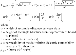
Table 1 [PDF format] shows some example values of the connection inductance associated with a decoupling capacitor for some typical dimensions. The more complex formula is more accurate, but even the simple rectangular formula values are accurate enough for most applications. The rectangular loop formula is
It is important to notice that the wire radius has very little impact on the loop inductance, and the height and width (area of the loop) has the major impact on the value of the loop inductance.
This type of analysis is also valid to decide if special board technologies, buried capacitance for example, is worth the cost for your board stackup configuration. If the buried capacitance layer is deep in the board (closer to the bottom), then the rectangular loop area between the IC power/ground pins and the buried capacitance layer will be high, minimizing any positive effects from the buried capacitance layer. Alternatively, if the buried capacitance layer is near the top of the PCB, the rectangular loop area associated with the connection inductance is small, resulting in the IC receiving the benefit of the buried capacitance layer without significant connection inductance.
There is no one correct answer to whether a decoupling capacitor should always be mounted on the top or bottom of a PCB. The best side of the PCB to mount the capacitor is the one where the rectangular loop area will be the least, resulting in the lowest inductance between the two options. PCD&M
Dr. Bruce Archambeault is an IBM distinguished engineer at IBM in Research Triangle Park, NC. He can be contacted at This email address is being protected from spambots. You need JavaScript enabled to view it..
REFERENCES
1. Wang, Chen, Jingkun Mao, Giuseppe Selli, Shaofeng Luan, Lin Zhang, Jun Fan, David J. Pommerenke, Richard E. DuBroff and James L. Drewniak, “An Efficient Approach for Power Delivery Network Design with Closed-Form Expressions for Parasitic Interconnect Inductance,” accepted for publication in IEEE Trans. on Advanced Packaging.
2. Knighten, J., B. Archambeault, J. Fan, G. Selli, L. Xue, S. Connor, J. Drewniak, “PDN Design Strategies: II. Ceramic SMT Decoupling Capacitors – Does Location Matter?,” IEEE EMC Society Newsletter, Issue No. 208, Winter 2006, pp. 56-67.


