New analysis tools measure the performance of the power delivery system and consider both cost and electrical performance resulting in a functional and cost-efficient design.
Power delivery system (PDS) design has become an important issue as power consumption of electronic products increases and internal power supply voltages decrease. As a result, design resources that were once exclusively reserved for signal integrity (SI) have now shifted to address power integrity (PI) issues. The most common way to address these PI issues is by adding decoupling capacitors (decaps). EDA vendors have now linked powerful analysis tools with PCB, package and IC design flows to consider PI issues.
Currently, the application of these tools is strongly focused on verifying the electrical performance of the PDS. This is a critical and necessary aspect of the design for release of prototype products or first mass commercial releases. However, heuristic-based design practices with subsequent verification tend to produce overly robust and unnecessarily expensive designs in which too many decaps are placed at too many locations. Expensive decaps are often selected even though less expensive components might serve equally well to meet performance specifications. Some designs apply only a single value while others apply a variety of decap values.
EDA PI analysis tools characterize the performance of a PDS by numerically simulating the high-frequency noise voltage between power planes. This noise voltage is a complex transient phenomenon that varies across the area of the PCB and is dependent upon all digital and analog signals for a given operating condition. It is impractical to consider this noise in detail for all possible operating conditions. Fortunately, it has proven successful for PDS design to instead examine the frequency-dependent input impedance to the power planes. The impedance referred to in the following discussion is the magnitude of the complex-valued input impedance and, therefore represents all resistive, inductive and capacitive effects in a single value. For a mounted component that low-noise DC power must be delivered to, it is practical to examine the impedance between the VDD and GND planes at its power pins. High values of impedance correspond to higher PDS transient noise levels. For a typical PDS the value decreases with increasing frequency for low frequencies, corresponding to the capacitance between the power planes. The impedance experiences a minimum and then begins to increase with frequency above this point, corresponding to the higher frequency inductive input impedance of the planes and the loop inductance of the planes in series with local decaps vias.
An optimum PCB design is one that minimizes impedance at the power pins of all noise-sensitive mounted components, at minimum manufacturing cost. At present, EDA PI analysis tools do not explicitly consider cost, nor do they perform optimization. However, a new PI technique has been created that considers both cost and electrical performance. An initial PDS design that includes decap placement and component selection is provided by the PCB designer. This new technique yields an updated design that meets a specified PDS impedance that can be manufactured at minimum cost. The technique provides a set of alternative designs that enable an analytical approach for considering cost-performance tradeoffs.
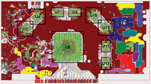
Implementing and validating this new PDS optimization technique requires the examination of several existing PCB designs – for example, a high-speed graphics board (Figure 1).
|

FIGURE 1. High-speed graphics card.
|
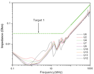
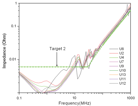
The PDS optimization for this graphics card simultaneously considers nine impedance values – one for the central graphical processing unit (GPU) and eight high-speed memory components surrounding it. The initial PDS design includes a single voltage regulator module (VRM) and 175 decaps. A total of seven different decaps are initially selected from a library of 24 unique components. The decaps in this library, or any subset of them, can be specified for use in the new optimized PDS design. The properties of these decaps include nominal capacitance, effective series inductance (ESI) and resistance (ESR), and physical size as well as component and placement cost. The PDS performance of the initial PDS decap design is represented by the nine impedance traces in the plot of Figure 2.
|

FIGURE 2. Impedance of all noise-sensitive components for initial PDS design with typical impedance target.
|
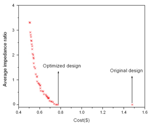
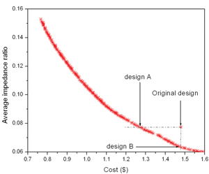
The total manufacturing cost of the decaps for this PCB is estimated at $1.48, inclusive of component and placement costs.
As for many high-speed products, the electrical performance of this PCB was more robust than required. A reasonable specification of maximum allowable impedance for the GPU and eight memory components is also shown in Figure 2. The new PDS decap optimization technique was applied to this PCB. The optimization adjusts the design with a goal of assuring each of the nine impedance values is less than the specified maximum allowable impedance. The PCB’s overall PDS performance is judged by what is called an average impedance ratio (AIR), which is a weighted average over frequency for all nine impedance values. In this case, the optimization is allowed to continue only until it achieves an AIR performance equivalent to the original design. The results of the optimization displayed in Figure 3 intuitively show PDS performance vs. cost.
|

FIGURE 3. Optimized PDS impedance vs. manufacturing cost.
|
The entire library of 24 unique decaps is available for placement at any of the 175 locations specified in the initial design. A placement constraint is enforced that disallows placement of a physically larger decap where a smaller decap initially was placed. The new optimized PDS decap design does not require placement of a decap at all 175 locations of the initial design. For this PCB, the optimized design required placement of only 87 decaps at a total manufacturing cost estimate of $0.77. This represents a savings of $0.71 per PCB, a $70,000 cost saving for the first 100,000 units.
In addition to a significant direct cost reduction, the PCB could potentially be examined for layout adjustments that would recapture the board area once occupied by the now unused decap pads and vias. For many products, this board area could be critically important to overall product size constraints. Elimination of these decap structures might allow for easier routing of traces within the same area, which could potentially reduce the required number of layers in the PCB stackup.
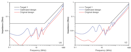
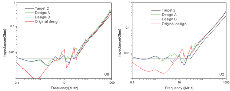
The impedance values in Figure 4 help establish a more intuitive understanding for the PDS behavior of the cost-optimized decap design vs. the original design. The plots correspond to the GPU (U8) and a typical memory component (U2). For the new cost-optimized decap design, the impedance values are generally larger than for the original design. This reduces the unnecessary robustness of the original PDS decap design. The PDS design objectives are achieved because the impedance values for the cost-optimized design are less than the specified maximum impedance over the entire frequency range. The AIR impedance plots shown in Figure 4 are provided as results of the optimization to enable analytical selection of cost-performance tradeoffs.
|

FIGURE 4. Impedance comparison between initial and cost-optimized design.
|
The same PCB with the same initial decap specification as before was again optimized. This time, a more stringent specification of maximum impedance was applied (Figure 5). This second optimization was allowed to continue to reduce the AIR performance of the PDS well below that of the original design. The objective was to find two alternate designs. Optimized design A is similar to what was examined previously: a design of equal performance relative to the specified maximum impedance. Optimized design B shows improved performance at equal cost. The original design and the two new optimized designs are shown in the AIR plot in Figure 6.
|

FIGURE 5. Impedance of noise-sensitive components for initial PDS design with aggressive impedance target.
|
|

FIGURE 6. Optimized PDS impedance vs. manufacturing cost for aggressive impedance target.
|
The impedance plots for these two new designs for the same components as shown before are in Figure 7. These impedance plots demonstrate two general behaviors of the optimized designs. First, unnecessarily low impedance values for low frequencies are not necessarily maintained from an original design for an optimized design. Second, it is important to observe a generally lower impedance level for this reduced maximum impedance specification, as reflected in both the AIR results and the impedance results.
|

FIGURE 7. Impedance comparison between initial and cost-optimized design for aggressive impedance target.
|
Specifying an aggressive maximum impedance results in better PDS performance. However, this better performance also corresponds to less cost-savings. Optimized design A results in a cost-savings for PDS decaps of $0.22 per PCB – a 15% reduction. Optimized design B results in better performance at the same cost. Figure 6 provides a high-level view of overall PDS performance, while Figure 7 provides a detailed view of the performance for each noise-sensitive component. In combination, this information enables analytical cost-performance tradeoffs to be made. Such analytical information is key to making effective business-level decisions.
The objective of an aggressive maximum impedance specification (as in Figure 5) is to improve performance beyond what optimization of the initial PDS design can accomplish. Figure 6 indicates a region of diminishing performance returns may exist for a cost greater than $1.60. The optimization technique changes decap components and avoids placement of certain decaps, but it does not move decap locations or add new decaps. The inductive frequency range above 10 MHz in Figure 7 does not significantly improve during optimization. This impedance behavior corresponds to a loop inductance comprised of local power planes and decap vias. Reducing this loop inductance improves high-frequency performance. The new PDS optimization technique already has selected decaps from the library to minimize this loop inductance as much as possible. The initial design could be changed to specify additional decaps near each noise-sensitive component, or existing decaps could be moved closer to those components. A PCB stackup change may be required to reduce the vertical separation between the power planes, which reduces the decap via inductances. Although the new PDS optimization technique does not automate such changes, it clearly determines when such modifications are needed to further improve PDS performance. After such modifications, the new technique should again be applied to assure minimum manufacturing cost.
One aspect of this PDS decap optimization technique that may not be immediately obvious is, at what stage in the product life cycle and by what type of engineer are performance vs. cost tradeoffs made? It is obvious such considerations can be made by a dedicated PI or SI engineer prior to manufacturing release for a new product. However, this PDS decap optimization technique does not require a high level of PDS design expertise, and can be performed by any PCB designer. The specifications are quite simple and the input is translated directly from an existing PCB CAD database. The GUI is relatively small, and has been crafted to be task-focused to support only PDS decap optimization and cost vs. performance tradeoff selection. In fact, a common application of these cost vs. performance tradeoffs is performed by manufacturing engineers after initial product release because, for many time-critical product releases, a short-term manufacturing cost can be tolerated to achieve target schedules. After initial release, substantial cost-savings can be realized without product re-design simply by selecting a different set of decap components.
This overview of a new PDS decap optimization technique has introduced an analytical manner in which to achieve significant product cost-savings. This new technique is invaluable for mass-production PCBs, for which a few pennies saved represents significant bottom line business impact. The commercial PCB design discussed here achieved $0.71 savings per board for reasonable PDS performance specifications, and $0.22 savings for an overly aggressive performance specification. The days of initial decap designs based on heuristics or vague design rules may not be gone, but this new optimization technique can help eliminate the high cost of unnecessarily robust performance. PCD&M
Brad Brim (This email address is being protected from spambots. You need JavaScript enabled to view it.) works in product marketing in the area of package and PCB extraction at Sigrity Inc.


