The use of simulation tools can improve the design process for embedded capacitor technology in high-speed and power distribution system designs where noise resonance reduction is critical.
The number of applications using embedded capacitor technology in PCBs is increasing. Some of these applications are high-speed digital systems and modules for hand held devices. For high-speed applications, design of power distribution system (PDS) is becoming extremely challenging. Good solutions for electro-magnetic interference (EMI) management are becoming very difficult to achieve as well. The traditional method utilized to cope with these challenges is the use of discrete capacitors. Improvement is gained by optimizing the type, amount and location of these components. As LSI technology scales to faster transistors and lower voltages, this traditional method is becoming ineffective, inefficient and costly. Embedded capacitor technology has proven to be effective in overcoming these issues by providing low impedance PDS and reduced EMI.
With respect to modules for hand held devices, the demand for improved higher density interconnects (HDI) is endless. One solution for HDI is to embed capacitor functions inside the PCB. Although there are various embedded capacitor materials proposed, the challenge still lies in the PCB fabrication to form uniform and reliable capacitors cost effectively. We will investigate designing embedded capacitor technology using commercially available simulation software.
Embedded Capacitors for High-Speed Applications
To incorporate embedded capacitors for high-speed digital application there are a number of different constraints that need to be considered. The first can be reviewed through power and ground noise simulation. Two of the major issues that electrical designers of high-speed digital equipment are facing are PDS and EMI. These phenomena are caused mainly by power/ground resonance noise. Simulation software to support electrical designers is available from various vendors. We have chosen EMIStream1 developed by NEC Corp. to investigate the impact of reducing power/ground resonance within a PCB that has embedded capacitors.
EMIStream simulation is based on a SPICE model and provides accurate simulation of power and ground resonance noise in a relatively short calculation time (around a few minutes per plane). The parameters that are required for the ground and power planes are dielectric thickness, dielectric constant and thickness of copper.
To determine the simulation results with discrete capacitor components, a board design for simulation was provided from NEC. The board is constructed from four layers, with the second and third layers being used as power and ground layers. The default design utilized 0.6mm FR-4 (Dk=4.6) with 1 ounce of copper on the power and ground layer. Thirty-five decoupling capacitor components (0.1µF) were mounted on the surface to supply power to the LSIs.
|

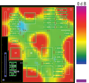
FIGURE 1. 0.6mm FR-4 (Dk=4.6) used as P/G plane (Red>0dB).
|
Figure 1 shows the power/ground resonance simulated result using a default design. The excitation point (source of noise) was chosen at LSI, indicated as U2 in Figure 1. The magnitude of noise level is listed as well. As you can see from the figure, there are areas where significantly higher noise has resulted from power and ground resonance. Areas higher than 0 dB are colored in red. With conventional methods of placing capacitor components on the surface, it is necessary to decide the type, amount and location of capacitor components. Figure 2 shows the result of placing a minimum amount of capacitor components to reduce the resonance voltage to below 0dB. Although it was possible to achieve 0 dB by adding 44 capacitor components (all 0.1µF), it was necessary to violate the placement location in the circled area of the figure. In this circled area, since LSI is already mounted, it is necessary to mount capacitor components on the backside of the board, which will cost additionally for surface mounting.
|

FIGURE 2. 0.6mm FR-4 (Dk=4.6) with 44 additional capacitors (Red>0dB).
|
Next, we have selected a set of embedded capacitor materials as listed in Table 1 to substitute as a power and ground plane to obtain simulation results. The embedded capacitor material has a thickness range of 8 to 24µm and Dk ranging from 4.4 to 30. This embedded capacitance material, FaradFlex, is commercially available and used in volume for high-speed digital applications. The detail material properties and processing are described in previous publications2,3.
First we conducted a simulation using parameters of BC24, dielectric thickness 24µm, Dk=4.4 (Figure 3). The result indicates that power/ground resonance can be reduced dramatically without any additional placement of capacitor components and achieve 0dB noise level. This implies that not only can a much lower noise level be achieved using embedded capacitor layers for the power and ground planes, but there is also a possible cost reduction by eliminating surface mount capacitors. In this case, a total of 44 capacitors were removed from this board, which is equivalent to 1,100 capacitors per square meter.
|

FIGURE 3. BC24 (Dk=4.4) used as P/G plane.
|
For certain high-end applications, achieving 0 dB is not enough. There are requirements as low as –26 dB noise level. This is due to lower margin allowance that results from the lower operating voltage of LSI. It is generally said that the allowed voltage fluctuation is 5%. This –26dB noise level is calculated by the following formula:
dB = 20*LOG(0.05) = – 26
Figure 4a shows the result with the default condition (P/G 0.6mm FR-4, Dk=4.6) with 44 additional capacitor components. The whole board area showed noise level of higher than –26dB. In this case, it was impossible to reduce noise level less than –26dB by adding capacitor components.
|

FIGURE 4. a) 0.6mm FR-4 (Dk=4.6) used as P/G plane; b) BC24 used as P/G plane; c) BC12TM used as P/G plane.
|
Figure 4b and Figure 4c show the result with BC24 and BC12TM used as power and ground planes without any additional capacitor components other than 35 default capacitors. With BC24 used in power and ground planes, it was possible to achieve –26dB noise level. With BC12TM in use, a much lower noise level was achieved. This result implies that in applications where very low noise levels are required, traditional placement of capacitor components is ineffective and the role of embedded capacitor technology becomes important.
|

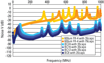
FIGURE 5. Maximum noise level at each frequency using different thickness of substrate used in power and ground plane.
|
In order to understand what properties of embedded capacitors affect the power/ground noise level, simulation was conducted to see the impact of dielectric thickness of embedded capacitor material. As shown in Table 1 [PDF format], by comparing embedded capacitor material with same Dk value and different thickness, BC24, BC16, BC12 and BC8, influence of dielectric thickness can be observed. In Figure 5 maximum voltage noise level in each frequency from 1MHz to 1GHz is shown. With 0.6mm FR-4 used in the power/ground plane it was difficult to achieve less than –5dB, even with additional capacitor component placement. When embedded capacitor material was used in the power/ground plane, -26 dB was easily achieved. It was found that the thinner the embedded capacitor material being used, the lower the noise level achieved. For instance, at resonance noise around 550MHz, the noise level of the PCB using BC24 was around –30dB, BC16 was –38dB, BC12 was –42dB and BC8 was –50dB. This implies that by selecting the appropriate thickness of embedded capacitance material, the target noise level can be achieved.
Another approach is to use higher Dk embedded capacitor material on power/ground plane. In Figure 6, maximum voltage noise in each frequency from 1MHz to 1GHz is shown. There are two sets of comparisons shown in this figure. The first set (Figure 6a) is a comparison between BC12 and BC12TM, in which both materials have the same thickness of 12µm but have different Dk of 4.4 and 10, respectively. Suppression of noise was observed with higher Dk material as well as the shift in resonance frequency. Figure 6b shows the second set of comparison between BC16 and BC16T, in which both materials have the same thickness of 16µm but have different Dk of 4.4 and 30 respectively. In this case too, with high Dk material, suppression of resonance noise and shift in resonance frequency were observed.
|

FIGURE 6. a) Maximum noise level at each frequency of different Dk material, BC12 and BC12TM used in power and ground plane; b) Maximum noise level at each frequency of different Dk material, BC16 and BC16T used in power and ground plane.
|
From these results we see that using higher Dk material has merit of reducing noise level and is useful to alternate the resonance frequency to avoid interference with specific frequency of interest without changing the thickness of power/ground plane.
RCF Type Capacitor Material and its Processing for Module/SiP Applications
One of the important issues of forming embedded capacitors for module application is uniformity of capacitance. This is particularly important when resin coated foil (RCF) is applied to module/SiP applications. To facilitate this there is a requirement for a practical and economical process using RCF type capacitor material. In one approach an RCF capacitor material is prepared by mixing high Tg epoxy resin with high Dk ceramic nano-powder and uniformly coating the mixed resin on the very low profile copper foil. It is supplied in B-stage as standard RCF for HDI application and it is very easy to laminate with core materials and to form a thin high-Dk capacitor layer inside FR-4 multi-layer PCB boards. Though it has relatively high ceramic content, the high Dk dielectric material shows enough insulation resistance, heat resistance and robustness required for standard PCBs. The material is also free from any halogenated substance to comply with current and any future regulations. It is available within a thickness range of 8 to 16 µm (with other thicknesses being evaluated). No special refrigerated storing condition is required other than the normal air-conditioned environment. An example of one material can be found in Table 2 [PDF format].
A thin and uniform high Dk dielectric layer is formed inside a PCB by laminating RCF capacitor on the core materials. However, in order to utilize this layer as singulated capacitors, we need to formulate the appropriate size of the capacitor to realize necessary capacitance, then electrically connect the capacitor with other devices and encapsulate the capacitor to protect it from various environments. To increase the rate of utilization of the board area and allow more freedom for board designers, removal of unnecessary high Dk dielectric is very important. There are several methods historically utilized to remove unnecessary resin in the PCB industry. They are laser ablation, plasma etching, dissolving by organic solvent and degradation by desmear solution. The authors have actually conducted several attempts with some of these traditional methods. The conclusion is that a sand blasting process (also called jet scrubbing or wet blasting) is the easiest, most economical and the most environmentally friendly process. Sand blasting machines are also very popular in the PCB industry for mechanical surface cleaning processes and many board shops are already equipped with them.
Figure 7 shows the process with sand blasting. As the curing rate of the high Dk dielectric is adjusted to be similar to FR-4 prepreg, standard FR-4 press profile can be generally used for the lamination process. The thickness of dielectric is substantially stable and unchanged during and after lamination, because the flow of RCF capacitor is minimal through the lamination process. Upper electrode is formed by the standard etching process, and the upper electrode acts as a mask while the board is being sand blasted. After sand blasting, lines and vias can be formed by the standard HDI process. As described, RCF capacitors do not require any special equipment or machinery to process; therefore we believe this is the easiest, fastest and most economical way to embed the capacitors inside PCBs and/or organic chip packages.
|

FIGURE 7. Capacitor embedding process using RCF capacitor material and sand blasting method.
|
For embedding singulated capacitors, one of the most important performance factors to be achieved is tight capacitance tolerance. Applications such as bypass capacitors may allow +/-20%, but applications for a filter circuit, for example, may require +/-5%. In order to achieve these tolerances, it is very important to understand how to control the tolerance of embedding capacitors.
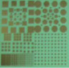
A test was conducted to investigate the tolerance of capacitors formed by using RCF capacitor material. Various sizes of capacitors, from 0.0625mm2 (250x250µm) to 4mm2 (2x2mm) were formed using the test vehicle shown in Figure 8. Capacitance measurements were conducted using flying probe capacitance measurement equipment from Hioki E.E. Corp. Measurement results are shown in Table 3 [PDF format]. Regardless of the size differences, all of the capacitors had less than 10% variation.
|

FIGURE 8. Capacitance pattern.
|
The tolerance of capacitance is determined by mainly two factors. One of the variations of capacitance is due to non-uniformity of the capacitance material itself, and another is variation associated with etching variation when forming electrode for capacitors. The total tolerance of capacitance can be expressed in Equation 1:.
Total tolerance of capacitance (%) = V1 (Capacitor material variation, thickness, Dk) + V2 (Etching pattern variation)
V2 can be expressed in functions of D (Target electrode size in mm) and d (Etching variation in µm) (Equation 2):
Expected tolerance of capacitance (%) = V1 (Variation by dielectric coating) + V2 (((D+d)*(D+d)-D*D)/D2/106*100)
With these equations, expected capacitance tolerance can be calculated depending on the size of target capacitor electrode and etching variation. Figure 9 shows the simulated results of expected capacitance tolerance in the case of +/-5% capacitance material variation. Each simulated line indicates variation created by a certain etching variation. In Figure 9, for instance, with the capability of etching patterns in +/-5µm (circle plot), it is assumed that +/-6% can be achieved when forming 1mm2 capacitors and +/-8% can be achieved when forming the 0.1mm2 capacitors. In the case of etching capability of +/-15µm (square plot), the expected tolerance would be worse, +/-8% for 1mm2 capacitors and +/-14% for 0.1mm2 capacitors. From these results, not only the uniformity of capacitance material is important to achieve tight tolerance, but also etching capability is important – especially in forming small size capacitors.
|

FIGURE 9. Simulation result of expected capacitance tolerance.
|
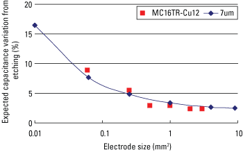
A test was conducted to compare simulated results and actual tolerances of capacitors in different capacitor sizes. The capacitor material used in the test was MC16TR with 12micron Cu. Figure 10 shows actual measured tolerance results from capacitance sizes of 0.0625mm2 (250x250µm) to 4mm2 (2x2mm). Actual measured capacitance tolerance matched quite well with simulated results using +/-7µm as an etching variation. This implies that the etching capability of the PCB manufacturer where this test board was fabricated has an etching capability of +/-7µm. In this case, +/-10% tolerance was achieved at a capacitor size as small as 0.0625mm2 (250x250µm).
|

FIGURE 10. Comparison of actual result with simulation result.
|
Each PCB manufacturer will have some difference in their etching capability. Once the etching capability of the PCB facility is known, it is possible to estimate what the expected tolerance of capacitance at each capacitor size will be using the calculation method described here.
For high-digital applications, usage of embedded capacitance in power and ground plane was proven to be very effective to reduce noise by the simulation software. As LSI speed increases and as operational voltages decrease, embedded capacitor PCB technology can offer an effective solution to meet the requirements. By using a simulation tool like EMIStream, electrical designers can easily understand the advantage of using embedded capacitors in PCBs to reduce power and ground noise, and to improve power distributions. The use of these types of simulation tools will help to accelerate the use of embedded capacitor technology for PCBs. For forming singulated type capacitors, we have demonstrated that RCF type capacitor material with a sand blasting process to form the capacitor is a practical, reliable and economical method. To form uniform capacitance, more than uniformity of capacitance material is important. Etching uniformity also plays an essential role, especially when forming small size capacitors. PCD&M
Kazuhiro Yamazaki is marketing director, Oak-Mitsui Technologies; John Andresakis (This email address is being protected from spambots. You need JavaScript enabled to view it.) is vice president of strategic technology, Oak-Mitsui Technologies; Fujio Kuwako is president, Oak-Mitsui Technologies. Yoshi Fukawa is president, TechDream.
ACKNOWLEDGEMENT
We appreciate Dr. Tint of HDI Solutions for his assistance with capacitance measurement.
REFERENCES
1. EMISTEAM Web site: www.emistream.com/product/product.html
2. TPCA 2004 Forum P52, T. Yamamoto et al.
3. IPC 2005 Technical conference, J. Andresakis et al.


