Accurate modeling of package inner structures aids high-speed system-level simulations.
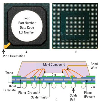
Modeling has been demonstrated to save time and improve efficiency in the design process. The modeling of plastic ball grid array (PBGA) package leads using TDR measurements in conjunction with IConnect software can provide valuable information for high-speed analyses. Figure 1 depicts three views of a PBGA package. The top view, Figure 1a, indicates that such packages are often marked with information related to device identification and manufacturing traceability. This includes1 the company logo, pin 1 orientation, device part number, revision, product family, lot number, date code, etc. Figure 1b displays the bottom view of a PBGA having 868 balls. The ball pitch for this package is 1.0 mm (39.37 mils). Other common PBGA pitch values include 1.27 mm (50 mils), 0.8 mm, 0.65 mm and 0.5 mm. The solder balls are simultaneously fastened to the host PCB to furnish an electrical path.
|

FIGURE 1. Three views of a PBGA package: (a) top, (b) bottom and (c) cross section.
|
PBGA is a popular surface mount choice for high I/O devices, offering numerous advantages2 over other high lead count (exceeding ~ 208 leads) packages. For instance, PBGA has reduced coplanarity and handling problems. The solder balls are self-centering (up to 50% off the pad) during reflow, decreasing placement issues.
The PBGA cross sectional view of Figure 1c illustrates that signal path from die pad to the solder ball can contain wire bond, package traces and via(s).
TDR measurements were performed to model such inner package topology.
Obtaining accurate models of package inner structure can be useful for high-speed system-level simulations.
Sometimes the raw TDR3 measured data of a Device Under Test (DUT) can prove sufficient for analyses (i.e., no need for post-processing). However, use of post-processing software such Tektronix (TDA System’s) IConnect can be quite effective in certain other applications, such as when extracting transmission line losses, fault isolation, or for modeling and SPICE simulations.
TDR measurements were carried out on a PBGA high-speed signal lead using Agilent 86100A Infiniium DCA wide-bandwidth oscilloscope mainframe with Agilent 54754A differential TDR plug-in module. A small probe of low tip inductance was utilized. The probe’s signal and ground leads were connected to PBGA’s lead of interest and an adjacent ground ball, respectively.
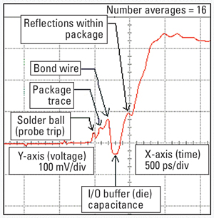
The TDR result (Figure 2) shows the locations corresponding to probe tip (solder ball), package trace, bond wire and die capacitance. The DUT TDR waveform plus measurements for short and open references were saved in Verbose text format. These TDR generated files were then modified (in the header sections, either manually or using Perl scripts) to make them compatible waveform files for importing into IConnect for post-processing operations. TDR data can also be transferred directly by interfacing the TDR oscilloscope, via GPIB or local oscilloscope interface, to the computer with IConnect software.
|

FIGURE 2. DR signature for a PBGA lead.
DR signature for a PBGA lead.
|
Models of package or PCB traces can be generated with IConnect in several formats, including: lumped RLC, single line (distributed), S-parameter Touchstone files, distributed lossy line and S-parameter based behavioral RLC models (highly accurate). The following paragraphs describe extraction of package model in the single line form.
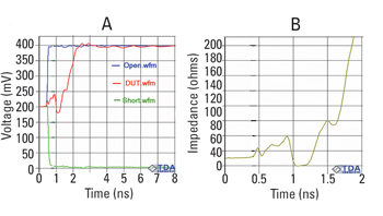
First the Z-Line impedance profile was computed. For accurate acquisition, the incident step (first transition in TDR waveform corresponding to interface from sampling head to cable) should be excluded4. An impedance deconvolution algorithm implemented in IConnect program de-embedes5 multiple reflection effects (in a multi-impedance DUT) and accurately computes the true impedance profile for each segment. The impedance profile of a DUT represents characteristic impedance as a function of distance along a device’s length. Figure 3a shows the DUT, open and short waveforms. Only one of the references (open or short) is required. A short reference may yield superior launch features, but an open, with nothing connected, usually produces more repeatable results. Figure 3a and Figure 2 reveal that the lead on the inside of package is open-ended. The DUT and open waveforms were applied to compute the Z-Line profile depicted by Figure 3b.
|

FIGURE 3. The DUT and the reference waveforms (a), and the computed Z-Line profile (b).
|
The peaks, dips and straight sections in an impedance profile correspond to inductive, capacitive segments and transmission lines6, respectively. The reference and reflection (DUT) waveforms were also utilized to extract a single line model4 of the PBGA package lead, consisting of a series of cascaded transmission line sections. The modeling was performed starting with measured voltage, rather than impedance, waveforms to allow IConnect to automatically build SPICE netlists for model validation. Open termination was specified since DUT was un-terminated.
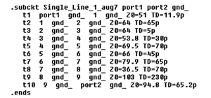
An IConnect-produced single line SPICE subcircuit is illustrated by Table 1. When producing such SPICE models, an effective approach is to start with automatic partitioning, followed by manual adjustments (partitioning) to enhance model accuracy, if necessary.
|

TABLE 1. IConnect-generated single line model segments for a package lead.
|
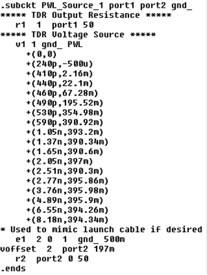
The open reference waveforms were also applied to create a piecewise-linear (PWL) source model shown by Table 2. This PWL source serves as an excitation model for launching an incident step into a DUT model; this facilitates model validation6 by ensuring that the source in the simulation and measurements are equivalent and any discrepancy between the measurement and model simulation are only due to the model.
|

TABLE 2. Section of an IConnect-produced PWL source.
|
The IConnect generated PWL source is a piece-wise approximation of the TDR source (based on the reference short or open waveforms) and accounts for effects of cable connecting the TDR and DUT. It is important to simulate the extracted DUT model and ensure correlation between simulation and measurement data.
The PWL source can be applied as input to DUT model for SPICE simulations. The TDR measured and simulation results for DUT can be then exported into Excel and plotted/superimposed for correlation analyses.
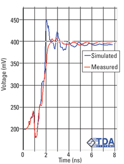
Alternatively, the Berkeley SPICE 3 (automatically installed with IConnect) can be linked for achieving quick/efficient comparison of the DUT TDR measured and simulated data. This approach was adapted to produce correlation result displayed by Figure 4.
|

FIGURE 4. The TDR measured (in red) and simulated (blue) waveforms superimposed.
|
To accomplish a good level of model accuracy, first automatic partitioning was applied followed by manual partitioning. Figure 4 indicates a close match between the measured and simulated waveforms in critical sections, but mismatch in the region of the open end. Improved correlation for the secondary reflections section may be also achieved by further enhancing the single line model via manual adjustments. PCD&M
Dr. Abe (Abbas) Riazi is a senior staff electronic design scientist with ServerWorks (a Broadcom company) in Santa Clara, CA. He can be reached at This email address is being protected from spambots. You need JavaScript enabled to view it..
ACKNOWLEDGEMENTS
My gratitude to Dean Gonzales, Mohammed Ishaq and Richard Kuo of ServerWorks, and Dima Smolyansky of Tektronix for helpful suggestions.
REFERENCES
1. “Device Marking Conventions,” National Semiconductor, July 2005.
2. “2000 Packaging Databook,” Intel. P. 14-1.
3. Abe Riazi, “TDR for Differential Pair Characterization, Part 2,” Printed Circuit Design & Manufacture, December 2005, PP. 30 -31.
4. TDA Systems IConnect Version 3.0 Manual, PP. 1-4 to 1-6, PP. 2-5 to 2-7, PP. 5-6 to 5-18, P. 8-6, P. 10-3.
5. Tom Granberg, “Handbook of Digital Techniques for High-Speed Design,” Prentice Hall, 2004, P. 529, P. 547.
6. “TDR Techniques for Characterization and Modeling of Electronic Packaging,” TDA Systems Application Note, 2001.


