Written by Andrew Mawer, Thomas Koschmieder, Paul Galles, Randy Anding, George Skevofilax and Tim Lippe
Category: 2012 Articles
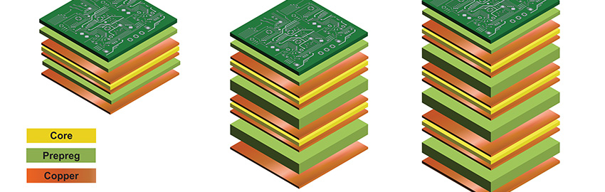
Underfilms have material properties similar to underfills but are easier to process.
A common failure mode for portable electronics is mechanical failure as a result of being dropped from sufficient height to cause damage. Most portable electronics producers qualify assemblies by performing some type of system-level drop test, while component suppliers typically utilize industry standard drop tests such as JEDEC JESD22-B111.1 It is well known that Pb-free solders do not perform as well in drop or shock testing as the Pb-free solders they replaced.
Much work has been carried out to optimize Pb-free alloys to improve drop test performance.2-6 Many companies have also implemented epoxy underfill to further increase robustness of the interconnection between the BGA and printed circuit board. These underfills are typically dispensed around the BGA following SMT assembly and electrical testing. Capillary action then slowly draws the underfill under the BGA. The underfill may be dispensed in sufficient volume to cover the entire BGA underside, the corner areas only or just the package sides. Finally, the underfill is cured in an offline batch oven. While excellent drop test results have been demonstrated with underfill, the process adds cycle time and may involve processes not normally performed during assembly. Another option for providing greater BGA to PCB mechanical robustness that may provide a more seamless integration into the SMT manufacturing process is the use of a preform underfilm material.7 The material can typically be provided in reels similar to discretes and is placed around the perimeter of the BGA following solder paste printing and prior to BGA placement. In reflow, the underfilm softens and initially expands such that it contacts both the BGA and the PCB. By the conclusion of reflow, the material fully cures, while remaining adhered to both the BGA and PCB.
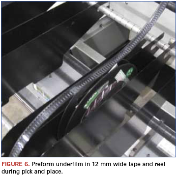
For our study, the preform underfilm material was a fully cured, low flow polyurethane polymer. It comes in a variety of shapes and sizes, and for this study it was specified in 4.0 x 0.76mm preforms with a thickness of 0.165mm. The preforms were provided in EIA-481-compatible 12mm wide carrier tape with a cover tape similar to how discretes would be supplied. The underfilm material is a thermoplastic designed to soften, flow and expand during reflow, thereby filling in the gap between package and PCB. Upon cooling in the reflow oven, the material resolidifies and bonds the package to the PCB. For this study, it was decided to use two of the preforms per corner, which effectively formed an L-shaped pattern. It should be noted that L-shaped preforms could also have been used.
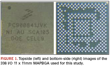
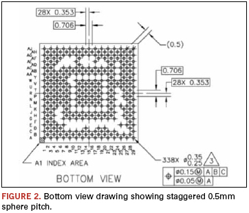
The test vehicle (Figure 1) was a 338 sphere 11 x 11mm body size PBGA with spheres at a staggered 0.5mm pitch (Figure 2). It is a package typical of portable electronics applications. The composition of the Pb-free spheres was SAC 105 (98.5%Sn, 1.0%Ag, 0.5%Cu by weight). The PBGA was molded all the way to the substrate edge in what is called a Mold Array Process (MAP).
The dummy die size inside the daisy-chain package was 5.3 x 5.4 x 0.28mm; the two-layer substrate thickness was 0.21mm, and the total package thickness excluding spheres was 0.92mm. The pads on the package were SMD with a specified 0.38mm copper diameter and a 0.30mm soldermask opening.
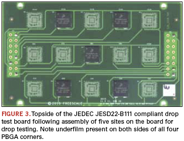
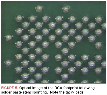
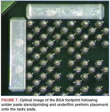
The test board used was based on the JEDEC drop testing specification for devices with less than or equal to a 15 x 15mm body size. The board (Figure 3) was 132 x 77mm and 1.0mm thick with eight layers of copper. The surface finish was OSP. SMD pads on the PCB were designed to exactly match the package, with a copper diameter of 0.38mm and a soldermask diameter of 0.30mm. The only modification made to the test board to accommodate the underfilm preforms was the addition of four additional pads in each corner of the package footprint. Once printed with solder paste, these tacky pads served as a way to keep the underfilm in place prior to reflow.
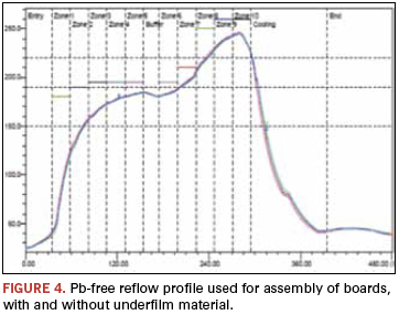
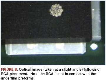
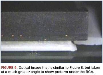
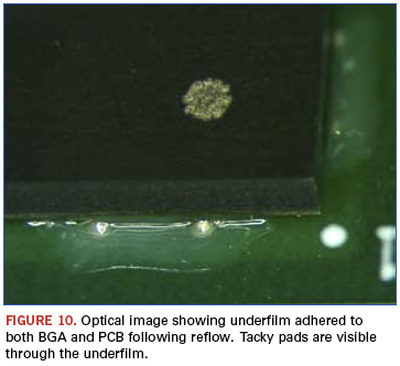
Assembly was carried out using a high-volume production SMT line with automated pick-and-place equipment and automated solder paste volume inspection. PBGAs were supplied in JEDEC trays. The Pb-free solder paste used was a halogen-free, no-clean with a SAC 305 composition (96.5%Sn, 3.0%Ag, 0.5%Cu). The reflow profile (Figure 4) had a peak temperature of 244.5º to 246ºC, depending on thermocouple location. Total reflow time was approximately six minutes. Each underfilm preform was placed on the two tacky pads near each corner of the part following solder paste printing. BGAs were then placed normally. Figures 5 to 10 show photos taken at various steps in the assembly process from printing and underfilm preform placement through BGA placement and reflow.
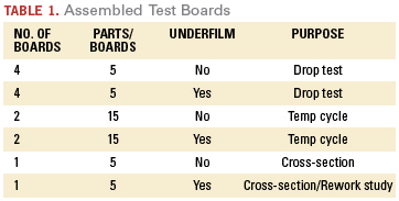
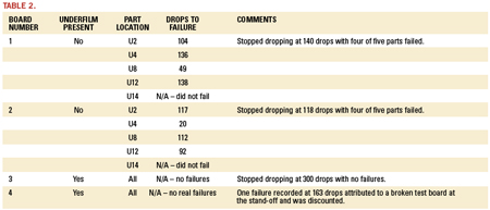
As shown in Table 1, a total of 14 boards containing 130 total components were assembled. On the boards for drop test, only five sites were populated (Figure 3). This is permitted by the JEDEC standard and was done to provide the most consistent drop test results by not populating parts close to corner standoffs. For the boards for thermal cycling, all 15 sites were assembled. Two additional boards were assembled for cross-sectioning. One hundred percent yield was achieved in assembly, and all underfilmed BGAs appeared to have the material adhered as expected between the BGA and the PCB in all four corners.
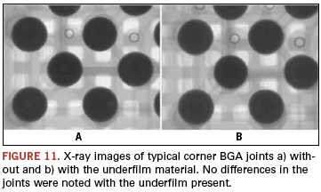
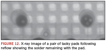
X-ray analysis. Following assembly, all boards underwent x-ray, with close attention paid to corner joints that may be in contact with the underfilm material. No misshapen or anomalous solder joints, such as those with opens, shorts, or excessive voiding, were observed (Figure 11). Additionally, the tacky pad locations were x-rayed, and all the printed solder paste was seen to be soldered to the pad, as opposed to being dispersed in the underfilm (Figure 12).
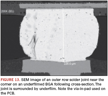
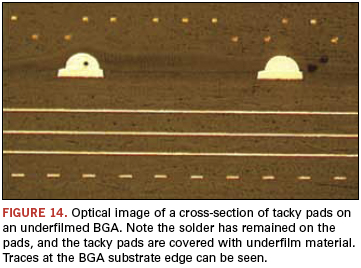
Cross-sectional analysis. Underfilmed and non-underfilmed BGAs were both cross-sectioned to the outer row to assess the solder joint formation and standoff (Figure 13). The underfilm was seen to be enveloping the three to four solder joints closest to the corner. The solder joint standoff between the underfilmed and non-underfilmed BGAs was found to be similar. A cross-section through the tacky pads on an underfilmed sample further confirmed that the solder paste reflowed and remained on the tacky pads (Figure 14).
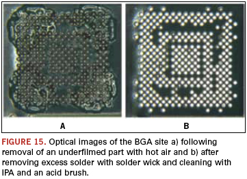
Underfilm rework evaluation. Using an extra board that was assembled with underfilm, a small study was carried out to ascertain the reworkability of underfilmed BGAs. Since the material softens at elevated temperatures, parts were removed using a hot air rework station using a standard rework cycle. A slight upward force was used to remove the BGAs once the Pb-free solder spheres melted. Excess solder was then wicked from the BGA pads and the entire area cleaned up with IPA and an acid brush. The resulting sites appeared to be underfilm-free and ready to accept another BGA (Figure 15).
Board-level thermal cycling. Boards populated with 15 parts per board were placed into thermal cycling, for a sample size of 30 parts with underfilm and 30 control parts without. The single chamber cycle went from 0º to 100ºC with 10 min. ramps and dwells for a cycle time of 40 min. or 36 cycles per day. As of this writing, the boards had gone 3,000 cycles with no failures in either group. This would far exceed most requirements for handheld portable electronics.
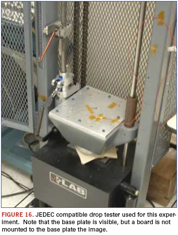
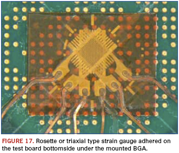
JEDEC drop testing. Drop testing was carried out using a JEDEC-compatible drop tester (Figure 16). During the drop, continuity to the daisy-chain parts was continually measured using a high-speed event detector. Additionally, triaxial strain gauges were affixed to the PCB on the bottomside of the BGA footprint to measure strain during the drop (Figure 17). Boards were attached to the base plate on the drop tester using four steel standoffs in the board corners. The JEDEC standard calls for boards to be dropped to Condition B, which is 1,500 Gs, as measured on the base plate with a 0.5ms duration and half-sine pulse.
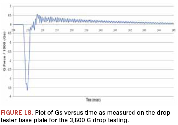
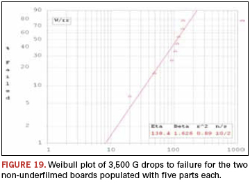
Two of the underfilmed boards and two of the non-underfilmed boards populated with five parts each were initially dropped 100 times at 1,500 Gs. No electrical failures were recorded on any of the four boards. It was decided to drop the remaining four boards to the maximum 120cm height on the drop tester to achieve failures in a reasonable amount of drops to enable assessment of the performance of the underfilm material. Dropping from this maximum height resulted in approximately 3,500 Gs being recorded on the accelerometer on the base plate. See Figure 18 for a typical accelerometer output during a 3,500 G drop. The 3,500 G drop also resulted in a maximum of approximately 1,500µm strain being recorded on the strain gauge under the mounted BGA. One non-underfilmed board was dropped 118 times and the other 140 times, resulting in four of the five parts failing on each board. The first of these failures was recorded at 20 drops. The number of 3,500 G drops to failure for these two non-underfilmed boards is plotted on Weibull axes (Figure 19).
One underfilmed board was then dropped 300 times at 3,500 Gs with no failures recorded on any of the five parts. The intention was to drop the other underfilmed board 300 times, but following 163 drops, a failure was recorded on one of the underfilmed BGAs. The test board was inspected and was found to have broken in the corner where it attached to a standoff. The part that recorded the failure was located in the broken corner. This failure was discounted, and drop testing was terminated at this point. If a true failure had occurred on this board at this point, the underfilm material would have increased the drops to first failure by at least eight times (20 versus 160+ drops) versus non-underfilmed parts. If this second board had not experienced a PCB fracture and experienced no failures out to 300 drops as the other underfilmed board did, the underfilm material would have provided a 15 times improvement in drops to first failure. All 3,500 G drop test results are summarized in Table 2.
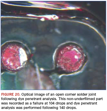
Drop testing failure analysis. A non-underfilmed part that had a failure at 104 drops was subjected to dye penetrant analysis following 140 drops.8 Typical solder joint fracturing was observed in the BGA corner (Figure 20). Since no true failures were recorded on any underfilmed parts, no analysis was performed on these.
Conclusions
A preform underfilm material designed to be a drop-in to the SMT process was evaluated for assembly characteristics, yield, drop test performance and thermal cycling reliability. The following conclusions were drawn from the study:
The preform underfilm material was seen to be a drop-in to a conventional, high-volume SMT process and was handled and pick-and-placed very similar to discretes.
Only a small design change was carried to the test PCB to accommodate the underfilm material. Tacky pads were added to the footprint to prevent any movement of the preforms prior to reflow.
One hundred percent SMT assembly yield was achieved with 21,970 0.5mm pitch joints formed robustly on 65 BGAs containing the underfilm material. Following reflow, all BGAs with underfilm appeared to have the material adhered as expected between the BGA and the PCB in all four corners.
The underfilm material had no observable effect on solder joint shape or standoff on the corner joints it came in contact with.
Using a JEDEC-based drop test at a severe 3,500 Gs, drops to first failure was increased by a minimum of eight times and probably much greater (15 times or more) with the use of the underfilm material. An exact improvement factor could not be determined since no actual drop test failures were recorded with the underfilm material.
Initial results suggest the underfilm material results in no degradation in thermal cycling performance. Thermal cycling to at least 50% failure continues.
Acknowledgments
The authors wish to acknowledge David Mendez and Kirk Kringel at Flextronics for technical and logistical assistance, Randy Temple and Dave Skupien at Alltemated for supplying the underfilm material along with applications assistance, Terry Burnette at Freescale for carrying out the rework evaluation, Scott Stoller at Freescale for performing the drop testing, Roy Arldt at Freescale for cross-sectional analysis and Ed Hall at Freescale for management support of this project.
References
1. JEDEC JEDS22-B111, “Board Level Drop Test Method of Components for Handheld Electronic Products”, July 2003, www.jedec.org. 2. C. Chiu, K. Zeng, R. Stierman, D. Edwards, and K.Ano, “Effect of Thermal Aging on Board Level Drop Reliability for Pb-free BGA Packages”, ECTC, p.1256, June, 2004. 3. D. Henderson, “On the question of SAC solder alloy – Cu pad solder joint fragility”, Webcast Meeting on SAC Solder Joint Fragility, Binghamton, NY, September, 2004. 4. S. K. Saha, S. Mathew and S. Canumalla, “Effect of Intermetallic Phases on Performance in a Mechanical Drop Environment: 96.5Sn3.5Ag Solder on Cu and Ni/Au Pad Finishes”, ECTC, S29p5, June, 2004. 5. M. Amagai, Y. Toyoda, T. Ohnishi, S. Akita, “High Drop Test Reliability: Lead-free Solders”, ECTC, S29p7, June 2004. 6. Alltemated Place-N-Bond Pick-and-Place Underfilm product data sheet, http://www.alltemated.com/img/Place-N-Bond-Underfilm-data-sheet.pdf?vsid=ypxrplzu. 7. W. Liu and N.-C. Lee, “Novel SACX Solders with Superior Drop Test Performance,” Proceedings of 2006 SMTA International, September 2006. 8. T. Burnette and T. Koschmieder, “Solder-Joint Failure Analysis”, Advanced Packaging, January 2003, pp. 25-27.
Ed: This article was first published at SMTA International in October 2011 and is reprinted here with permission of the authors.
Arraying boards reduces panel cost and speeds assembly.
What do you think of when you hear the word “array”? Perhaps an antenna array, or possibly some type of mathematical array, or maybe even video graphics array (VGA, such as the adapter connection from a PC to a monitor)? It is one of those words that can mean something different to almost anyone who hears it.
Questions about arrays are very common in PCB manufacturing. An array combines a single PCB multiple times to make a larger group of connected boards. This process is sometimes referred to as “stepping out” the individual boards, or “step and repeat.” Other terms used to describe an array are panelized, stepped out, palletized and route and retain.
An array helps an assembler with the build process. Parts can be loaded at a much faster rate because the manufacturer can assemble the entire array at one time, instead of loading one board at a time. Boards are loaded using automated pick-and-place machines, which pick up parts (normally surface mount devices) and place them on the board.
Paradoxically, arraying boards will typically raise the cost of individual boards. This happens because fewer panels are used when boards are in an array versus when they are processed as individual boards. Although the individual board cost will rise, however, the cost of board assembly is less because of the array configuration.
General Guidelines
Each electronics assembler and manufacturer will have their own specific guidelines of how they would like to have their arrays set up for manufacturing. These guidelines provide some ideas of general practices that are fairly typical for most.
Array size. Typical sizes are 8 x 10" or 10 x 12" as the overall largest size of the array. If the PCB manufacturer is using a production panel size of 18 x 24" with a usable space of 16 x 22", then the best fit of the largest array will be 7.8 x 10.8". That will permit at least four arrays “up” on the panel. If the array size is larger than that, only two arrays will fit, and the cost per board will go up significantly. Smaller array sizes can be used for smaller individual boards and still have a good yield for each panel.
Rails. Rails are extra PCB material added to the sides of the array to permit easier handling during assembly. Rails could be on two sides or all four sides of the array. Restricting rails to two sides usually permits a few more pieces on the panel, which helps the per board cost.
Fiducials. Typically three fiducials are needed on an array, and they usually go on the rails. The ideal size is 50 mils. The fiducial is a circle that is a copper pad with the same finish as the rest of the board on it. This provides alignment targets for the automated assembly equipment to get things lined up. Some manufacturers may require fiducials on each individual board as well. However, for the most part there are pads or other features on the individual boards that can be used to provide additional alignment targets.
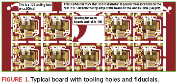
Tooling holes. Tooling holes in the four corners of the array in the rails is fairly common as well (Figure 1). Again, these are used to aid alignment and orientation when assembling the board. The typical size is 125 mils, and they are non-plated.
Array spacing. Spacing depends on whether the array is scored or routed. For tab route, the spacing is 100 mils in most cases. With scoring, the boards can be placed next to one another with no spacing. Those also are the two options for “depaneling” (separating) boards after assembly.
Scoring. Scoring is the act of making a small “V” groove along the length of the board where separation takes place (Figure 2). The groove is typically one-third on top and one-third on bottom, leaving one-third of the material in place to hold the boards together.
When scoring, there should not be any parts placed within 250 mils of the edge of the board. If they are closer than that, there is the possibility that the parts could come loose during the depaneling process. If the board thickness is more than 62 mils, and the score line is a long score line, it can require a significant amount of force to separate the boards.
Tab Route. Tab route arrays will leave a small tab on all four sides of the board attached to the other boards or the rails. This type of array is not as stiff as the scored array but can be easier to break apart.
Tabs are typically one on each side of every board and usually 50 mils wide. They usually have small holes drilled on the edge of the tab at the board outline. Those small holes are referred to as mouse bites or perforated holes, or sometimes rat bites. Either way, they make it easier to break tabs off the board. They do leave a rough edge, so additional sanding or grinding might be needed for smoothness.
X-outs. An X-out is when one of the individual boards on the array does not pass test and is marked out usually with a marker. Some manufacturers will permit a certain percentage of X-outs (such as 10%) on the order, while others may require no X-outs on any of the arrays. No X-outs will make the board a little expensive, since the PCB manufacturer may need to make a larger number of arrays in order to meet the order requirements, depending on their yields.
Calculating Array Size
Many manufacturers use automated programs for calculating arrays. Here are the steps to getting a best fit array using one such program, called KwickFit.
Set panel size at 18 x 24" with 1" margins (or whatever the panel options are for whichever firm is manufacturing the PCBs) (Figure 4).
Select define array. In the Array Definition area, enter the individual board dimensions (Figure 5).
Max. size of 7.8 x 10.8"
Min. qty. of 1, max. qty. of 100
Click calculate.
Using these settings, the tool will output the most number of possible boards up on the full panel and on the individual array. This works well for the majority of board sizes, up to about 4 x 4". Above that size means creativity is in order to come up with the array. Assume the largest x dimension will be 7.8 and the largest y dimension will be 10.8. Use the smallest dimension of the individual boards as the x dimension. (This also can be performed manually. A spreadsheet or a calculator makes this easier, of course.)
Step 1. Determine rail size. If the rail size is 0.5, double that (rails on both sides) and then deduct that from the total available dimension for the x dimension. That would then be 1" deducted from 7.8" = 6.8". That is the “usable” space for the array in the x dimension.
Step 2. Add your spacing to the size of the board. For example, the board is 1" and the spacing is 0.1". Added, that’s 1.1".
Step 3. Determine how many will fit. Divide 6.8 by the individual board size with the spacing added. In this case, 6.8 divided by 1.1 = 6.1. So six boards of 1" size fit in the x dimension using 0.1 spacing with 0.5 rails.
Step 4. Add together. Note: Because there are spaces on both sides of the boards, add 0.1 to the total of the boards to get the correct overall dimension.
The total for the x dimension is 6 pcs. * 1.1 = 6.6 + 0.1 (for the extra space) = 6.7 + 1 (for rails) = 7.7" in the x dimension
Perform the same process for the y dimension.
10.8 – 1 = 9.8" usable space 9.8 / 1.1 = 8.9 (rounded down), or 8 wide in the y dimension 8 * 1.1 = 8.8 + 0.1 = 8.9 + 1 (for rails) = 9.9" in the y dimension.
The result is 6 x 8 up (48 pieces) and the overall size will be 7.7 x 9.9 with 500 mil rails and 100 mil spacing.
This can be calculated manually as shown here, or by using an array calculator (such as at bayareacircuits.com/pcb-array-calculator/), which makes the calculations and provides a graphical image (Figure 6).
Peter Brissette is head of PCB sales and marketing at Bay Area Circuits; This email address is being protected from spambots. You need JavaScript enabled to view it..
The window to identify and train the next generation of designers is closing. What we can do about it.
Has anyone seen the next generation of PCB designers?
This was a rhetorical question posed by then-editor Kathy Nargi-Toth in PCD&F’s 2007 salary survey (December 2007). The response: a collective silence, at least until someone whispered, “No, we have not seen them,” because for the most part they don’t exist.
Most readers probably quickly continued to read the article to see whether, based on the national average, they should request a raise. Given that answer (“No, we have not seen them”), they all probably got one. For the record, the average age of a printed circuit board designer in the US is in the mid-50s; a fair number will be retiring within the next five to 10 years.
There are many experts in our field of PCB design, but are there many leaders? A famous quote may help us answer that question: “If you think you are a leader, look behind you to see if anyone is following you.”
Many of us have been fortunate to have worked in this chosen profession for many years, and we wish to thank all those before us who apprenticed, mentored, and trained us. Design is a great profession and rewarding on many fronts: technical knowledge, job satisfaction and a high-paying professional income. We’re hoping to inspire the reader to consider what part we can each play to bring into the industry the next generation of PCB designers.
To begin, we attempted to consider all different perspectives of those who might read this, and admit it was a difficult task. Our point is not to cast blame or aspersions against any individual or group. It is our assumption that most people and industries typically seek what is in their best interests and then act accordingly. Unfortunately, sometimes that may mean long-term good is sacrificed for short-term need.
This idea was reinforced at a recent industry meeting in San Diego in February, where a presenter asserted that “price is what you pay in the short term, and cost is what you pay in the long term.” His point was that saving on the price may cost much more in the long run. Our field of PCB design is about to experience this phenomenon. Can you imagine one day in the not-too-distant future where an engineering manager will go to work only to find the entire PCB design department has retired and there is no one to take their place? The time to recruit, train and develop the new PCB designer won’t be then. Rather, the time is now.
We will share some opinions and some observations in an effort to understand how our industry ended up in this situation. We’re sure you may be able to find exceptions to our opinions and experiences but please don’t discard the general concept we’re trying to convey. The only way we are bound to repeat history is to not learn from our mistakes.
Getting Into the Field
Most PCB designers entered the business from the drafting or technician field or from a friend’s reference. There are few college programs and fewer, if any, PCB degrees that you can get as an entry to the profession. Once in the PCB design profession, there are several training and development programs to pursue, and we encourage everyone to do so. As a manager of PCB designers, there is one trait that is looked for specifically. We call that trait “detailed packaging skill.”
It looks like this: When friends are moving and they ask for my help, they do not want me carrying their belongings to the truck. Rather, they want me inside the truck making sure that everything fits and has the best chance of remaining safe and secure during the ride. This distinction is what makes PCB design not just a trade but a skill. Many engineers have attempted PCB design because they comprehend much of it, but eventually concede that it may not be a skill they inherently possess.
From a historical perspective, when many people entered the profession, they came in as test technicians, trainees or junior drafters/designers. They learned using the system of OJT, or on-the-job training. They often worked in a large group, with a coworker assigned to mentor, train and develop them into competent designers. Eventually, they were released to perform tasks that steadily grew in responsibility. They then continued their career development using industry training, seminars, certifications, etc., but the main ingredient was mentorship.
What then occurred was industry downsizing, outsourcing and moving jobs offshore. The bulk of work was left to the few senior designers left standing; they would be asked to do it all. Not many new people were being brought into the industry. The remaining senior designers could demand a higher wage, which was our right. This development was exacerbated by some software vendors that saw the shortage of PCB designers and attempted to fill the gap by persuading the engineering community that they could just buy their software product, eliminate the PCB designer and push the “EASY” button.
As nearly every PCB designer is now sarcastically saying under their breath, “How’s that working for you?” The simple truth is the majority of engineers do not perform PCB design frequently enough to truly become consistently good at it, nor do they have the knowledge to design PCBs within the constraints of manufacturing requirements. Frankly, they really don’t want to be PCB designers. Forgive what may appear to be a rant, but we all have probably played a part in this situation of the shortage of PCB designers.
Where Do Designers Fit within the Enterprise?
If one surveyed every PCB designer whether they thought their position was valued and esteemed within the electronics industry, the overwhelming response would likely be “no.” We perform a function that everyone wishes could be eliminated. To qualify our position, consider the following: Do you view PCB design as an asset or a liability? If an asset, you would want to give this function all you could to make it successful and esteemed for those involved. If a liability, you would take away resources and not esteem those involved. Most of us would say we are doing more with less and often disrespected as professionals.
So, we ask, why would we want to bring someone into the field of PCB design? Why not just collect higher wages and ride into the sunset of retirement? After all, the corporate world had no concern for me during the downsizing, outsourcing and migration of jobs elsewhere. Some software vendors often seemed to want to sell the tool to the engineer to just bypass our discipline of PCB design.
These may seem like reasonable conclusions, but we find them short-sighted and possibly damaging to our conscience. What guides business are the very real concepts of profits and losses, and not necessarily common sense. In that vein, we offer for consideration some simple dollar-and-cents reasons.
The senior designer can manage and utilize an apprentice to accomplish an increased workload greater than what they are currently taking on by using what we call “hands 3 and 4” to satisfy the more simple tasks of silkscreen, documentation, simple routing, cleanup, etc. This allows the apprentice to develop as they observe the mentor’s work methods and seek to emulate them. To that end, a designer would be able to provide more value to their company by meeting the commitments of increased production with accuracy, quality and cost savings. Meanwhile, the company would be securing the next-generation of PCB designers by passing on the internal methods and procedures it currently utilizes. It would not need to reinvent the wheel and suffer the consequences of not having this department staffed, which often leads to outsourcing and offshoring, followed by a loss of quality and control. It would also realize the cost benefits of two designers at the cost of 1.5, guided by one senior designer.
Developing New Designers
You may ask, How should we develop PCB designers now so that they are of value to everyone concerned? We look for candidates with the skill-set mentioned earlier: packaging and attention to detail. They also should have an in-depth understanding of computers and knowledge of electronics. Then we observe their interpersonal communication skills. Places we would recommend to look for these types of candidates would be trade schools such as ITT Tech (itt-tech.edu) or local community colleges. As employers we then offer to them a temporary-to-permanent position to observe them for a few months. We assign them to a senior designer and let them support the senior, doing the repetitive, lower skill-level work until they master each assigned task and are ready for the next one on the “OJT” ladder. We eagerly encourage and support them to pursue any and all means of training, education and industry involvement. We continue to assess their progress and observe where they are succeeding and where they may be struggling. A continued development path should always be kept in front of them or they stop maturing as a PCB design professional.
And to the software vendors: We are grateful for the tools you develop for us, including those that permit real-time collaborative design, regardless of location. We challenge you to continue to get the software into colleges and trade schools to increase your user base, expose your product and invest in our industry.
For the time being, we have the skills to train and develop the next generation of PCB designers. We should take advantage of this limited opportunity, before the window closes. The simple incentives to value this discipline of PCB design are in our collective interest. You are the leaders of today. Let’s get someone to follow in your footsteps for tomorrow’s benefit. Please share this perspective within your company and within the electronics industry.
Michael R. Creeden, CID+, is CEO of San Diego PCB Inc. (sdpcb.com), a PCB design service center; This email address is being protected from spambots. You need JavaScript enabled to view it.. Jeff Kuester, CID+, is an application engineer at Mentor Graphics (mentor.com); This email address is being protected from spambots. You need JavaScript enabled to view it..
Neck-downs and vias are common “choke points” for current, but there are design solutions.
PCBs get hot. This is especially true of modern PCBs, packed with power-hungry ICs dissipating more heat than ever. But heat generated by the ICs isn’t the only consequence of their thirst for amps. The power distribution network, or PDN, must be designed to provide adequate DC current-carrying capability; otherwise additional heat can be generated on the board itself.
It is difficult to design a PDN that meets the high current demands of today’s ICs. Not only has the amount of current increased, but so has the number of different voltages used by the ICs. This means that power planes have to be segmented into multiple different islands, and trying to piece together all those different islands can often lead to neck-downs in the plane shapes. Additionally, lower voltages are being used – some less than 1V – which means there is very little margin for any voltage to be lost due to resistance in the PDN. And, of course, there is pressure to lower PCB costs, which limits the number of plane layers used in a design.
Common problems associated with inadequately designed PDNs include voltage drop, excessive current in vias, and excessive current densities in some area of the board. Drops in voltage can result in insufficient voltage at the IC power pins, which can lead to IC malfunction. Excessive current densities can lead to board damage and disconnected power in extreme cases, but will also result in board heating. Heating of the board by the PDN contributes to the overall heating problem on the board, and can reduce IC life.
These types of issues can be pinpointed and eliminated during the design phase through the use of analysis tools. One of the types of power integrity simulations performed is a DC drop analysis, or IR drop analysis, so named because it simulates the drop in DC voltage caused by current (I) traveling through the resistance (R) of the planes. Power planes can be mapped out in the pre-layout stage, or completed PCB designs can be analyzed to pinpoint possible neck-down areas, such as the area shown in Figure 1.
Such areas of high current density need to be eliminated, and these areas aren’t confined to neck-downs in the planes. Vias are another common “choke point” for current. Knowing how many vias to use to transfer power from one layer to another, or to connect a voltage regulator module (VRM) to the rest of the circuit, is not always intuitive.
Thermal analysis. It is also not straightforward to extrapolate temperature rise from a given current density. Many variables affect how the heat will dissipate, and the resulting temperature rise for that location. For instance, the method of connection of the “hot spot” to the rest of the plane is a large factor. Copper conducts temperature, not just electricity. Also, the percentage of metal in the surrounding layers above and below this area, as well as the board environment, will affect the temperature. These are the types of factors included in a thermal analysis. By performing a thermal/IR drop co-simulation, these hot spots in the planes can be examined for precisely how hot they will get.
Thermal simulations model all three methods of heat transfer: conduction, radiation and convection. Heat is conducted from the ICs through their pins and then throughout the board. Heat is radiated from the ICs and from the board. Heat is also transferred through convection – naturally, opposite the direction of gravity, as well as through forced convection if there is some type of fan or blower in the system. When a high current density area exists in a PDN, it acts like another heat source, and that heat gets dissipated by a combination of these three methods of heat transfer.
Voltage drop and temperature are actually closely related, because the resistance of copper changes with temperature. In fact, copper conductivity changes 4% for every 10˚C of temperature change. A temperature range of 80˚ equates to a 32% change in copper conductivity, which is quite significant. As such, to determine the actual current densities in the copper on the board, the temperature of the board must be known. And in order to determine the temperature on the board, the current densities on the board must be known. Hence, there is a need for a co-simulation between IR drop and thermal analysis in order to generate accurate results.
So, to accurately predict the temperature rise caused by areas of high current density, the temperature of the board must first be known. This requires, at the very least, modeling the power dissipation of the components, their connection to the board, the board itself, and the environment the board is in. With this information, thermal simulation can be used to develop a thermal profile of the board, which can then be fed into an IR drop simulation to ensure the appropriate copper conductivity. The results of the IR drop simulation can then be fed back into the thermal simulation to include the effects of power being dissipated by the PDN, and this back-and-forth iteration of simulations can continue until the simulators converge on a solution. An example of such a simulation is shown in Figure 2.
This simulation includes the heating effects of a 1.5V plane that is feeding two larger ICs on the right side of the board. Thermal effects are a little different from electrical effects in that it is much more difficult to isolate them. Electrical effects can be examined on a per-net basis. For example, a single signal net can be examined for signal integrity, or a single power net can be examined for power integrity. In thermal analysis, the entire board, including its environment, needs to be analyzed at once. As such, for maximum accuracy, all the power nets on the board, including the ground net(s), should be analyzed at once, since they all interact. In this example, more clearly depicted in Figure 3, there is obviously an area of increased temperature on the board corresponding to the area of high current density on the plane. Comparison against a thermal-only simulation reveals the importance of including the heating effects of the PDN.
More important, the heating effect of that plane shape neck-down is accurately characterized, and provides valuable information in driving a design change on the board. In this instance, the easiest solution would be to eliminate that neck-down on the plane shape. However, if that plane is feeding multiple voltages throughout the board, that may be difficult. Another solution may be to add another shape on another layer to help “bridge” the gap where the neck-down occurs, and stitch it to the existing plane shape using vias. Such a fix could be analyzed by performing another simulation.
Other hotspots. It is important to note that such plane shape neck-downs aren’t the only PDN design issues that can cause thermal problems. On any design with BGAs, especially finer-pitch BGAs, such problems will naturally occur in the breakout area beneath the BGA. There, the power planes are often perforated with antipads from signal and ground vias, forming a narrow web of copper to feed current to the power pins. These areas are commonly areas of very high current density, which can cause the same type of heating issues (Figure 4).
These areas can be especially problematic because they are already the highest temperature areas on the board, because they reside beneath the ICs. The ICs are typically the most significant sources of heat on the board, and the areas beneath them tend to be the hottest areas on the board as a result. Adding additional sources of heat to these areas – areas of high current densities caused by perforated planes – leads to higher temperatures on the IC and ultimately reduced component lifespan. For every 10˚ above 100, the mean time between failure (MTBF) of a component is reduced by as much as 50%.
Power pins and stitching vias can be another area of the design at risk for thermal issues. It is important that any VRM attached to the power planes be attached with adequate power pins and/or stitching vias, so that the current is distributed and temperatures of those pins and vias are kept relatively low. The same is true for vias stitching multiple power planes together.
Thermal issues are often solved in a variety of ways: adding heatsinks to components, changing airflow, or separating hotter components, to name a few. Thermal issues caused by inadequate PDN design have one simple solution: add more metal. This may mean widening traces carrying significant current, eliminating neck-downs from plane shapes, using thicker copper on the planes, or adding more stitching vias where necessary. The solution is simple. Through analysis of the power distribution system prior to building the boards, such problems can be quickly identified and resolved. This will result in designs that are more reliable and last a long time.
Patrick Carrier is product manager, high-speed PCB analysis tools, Mentor Graphics (mentor.com); This email address is being protected from spambots. You need JavaScript enabled to view it..
The month of May is quickly winding down, and the June trade show season is fast approaching. On June 13, the JPCA Show will open its doors at Tokyo Big Sight. The three-day event is the largest trade exhibition for the printed circuit industry. Most agree that the JPCA Show is always a great source of information for both technical and business tidbits. However, in my opinion, it is a great source of information to predict the future for the Japanese printed circuit industry.
Let’s first look at some data for the last eight years. Listed below are the annual revenue numbers for the Japanese PCB industry (provided by METI), as well as the percent change from the year below:
Growth rates were positive year over year from 2004 – 2007. There was a big hit to revenue during 2008 and 2009 at the peak of the global recession. Markets in every country suffered during this period of time. The printed circuit industry did recover nicely during 2010 and posted a 15% increase over 2009. The entire industry did not get caught up in the recovery wave, so analysts predicted slow and steady growth for 2011. Unfortunately, this did not come to fruition. Not only did revenue fall by 15% compared to the previous year, the industry also posted its lowest annual revenue in eight years. The bad news for the Japanese industry is this double digit negative growth did not happen in Taiwan, the U.S. and Germany. Taiwan has set new revenue records for this same period of time, and the U.S. and Germany are showing small but positive increases.
Most business analysts from the Japanese printed circuit industry recall the business environment in the U.S. after the IT bubble crash in 2001. The U.S. PCB industry suffered significant declines, and most of the larger sized circuit manufacturers quickly disappeared from the industry. The IPC Apex Expo is a large trade show for industry and attracts worldwide audiences. Participation dropped dramatically in 2002, and the show never recovered.
I think the JPCA Show 2012 will be very positive and upbeat. I do not think I will see any signs pointing to an industry melt down. However, I will be able to network and gather market information by communicating with the industry experts and management teams during the show. Some of this chatter that I can pick up during the show is a more realistic outlook for the industry in the upcoming year. I look forward to sharing some of these opinions in one of the upcoming newsletter.
Dominique K. Numakura DKN Research, www.dknresearch.com
Headlines of the week (Please contact This email address is being protected from spambots. You need JavaScript enabled to view it. for further information of the news.)
1. Asahi Kasei (Major chemical company in Japan) 5/14 Has started the construction of the new manufacturing plant in China for the photo dry films of PCB with an annual capacity of 120 million square meters.
2. Mirie Automation (Equipment manufacturer in Taiwan) 5/15 Has been getting a lot of new orders manufacturing equipment from Chinese LCD manufacturers for 5G, 6G and 8G lines.
3. Bridgestone (Major tier suppler in Japan) 5/15 Has decided to close the e-paper business because of extreme price competition in the market. The manufacturing will be terminated by October.
4. Panasonic (Major electronics company in Japan) 5/15 Has rolled out a new 65” size white board with PDP technology for business use. 85” and 103” size products will be commercialized by the yearend.
5. Nippon Electric Glass (Major glass material supplier in Japan) 5/16 Will open a new manufacturing and marketing subsidiary in Korea for the local customers of LCD glass substrates.
6. Furukawa Electric (Major cable manufacturing company in Japan) 5/17 Will ship out the first high voltage (275 kV) super conductor cable from Ichihara Plant. Its field test will be conducted in China.
7. Ricoh (Major electronics company in Japan) 5/21 Has developed a new lead free piezo material applying inkjet printing process of PZT for actuator devices.
8. Kobelco (Major steel supplier in Japan) 5/23 Has developed a new fuel cell separator material by coating carbon material on titanium. It reduces the contact resistance to half compared to the other metals.
9. Sharp (Major electronics company in Japan) 5/24 Had agreed to have a procurement alliance with Toppan Printing and Dai Nippon Printing for the color filter materials of LCD panels in Sakai Plant.
10. New Japan Radio (Device manufacturer in Japan) 5/24 Has established the first volume production process of the copper wire bonding on aluminum pads for power semiconductor chips.
DKN Research Newsletter May 27, 2012 (English Edition) Electronic Packaging Industry News from Japan & Asia (www.dknresearchllc.com)