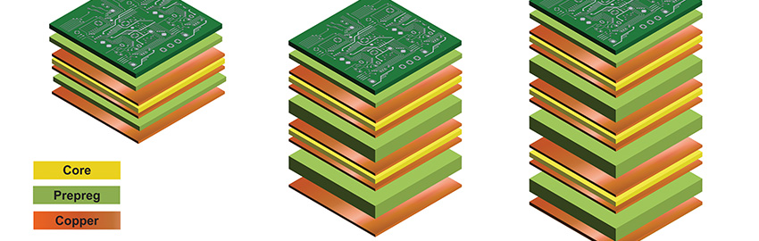
The 104 manufacturers on the 2011 NTI-100 made up more than 80% of the world’s PCB output.
The NTI-100 list for 2011 was greatly influenced by exchange rates. Taiwanese fabricators continued to make gains, followed by Japanese manufacturers. Some names disappeared because they were purchased; their sales are included in the acquiring firm’s results. Some disappeared because they did poorly. Several fabricators, particularly Japanese firms, made it because of exchange rates.
As usual, the author is not almighty and is certain that there are many errors. Some companies that should be on the list may be missing. He assumes full responsibility for any errors. He wishes to express his gratitude to those PCB makers that provided him valuable data.
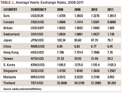
Exchange rates. Currency values played a role in certain companies’ performance. Table 1 lists the average exchange rates of major currencies against the US dollar.
Assumptions. All acquisitions that took place during 2011 are assumed to have taken place on Jan 1, 2011. In the cases of flexible circuit manufacturers (FPC), the assembly value is included because it is extremely difficult to separate bare board sales from total revenues. Therefore, the rankings are relative, not absolute. Finally, a large portion of revenues of Taiwan, Japanese and US makers comes from overseas operations, and therefore involves double conversions. The author has no knowledge of what exchange rates Taiwanese makers, for example, used to convert output in RMB into NT dollars to report consolidated revenues.
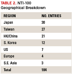
Entries by country or region. There are 104 companies on the 2011 NTI-100 list. There are more Japanese makers than Taiwanese because of a 10% increase from 2010 to 2011 in value of the Japanese yen against the US dollar. Several Japanese makers would not have made it had the 2010 exchange rate remained constant.
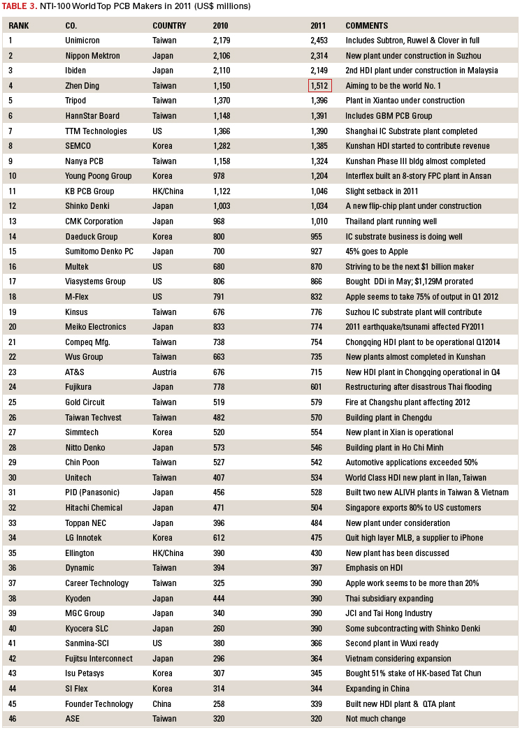
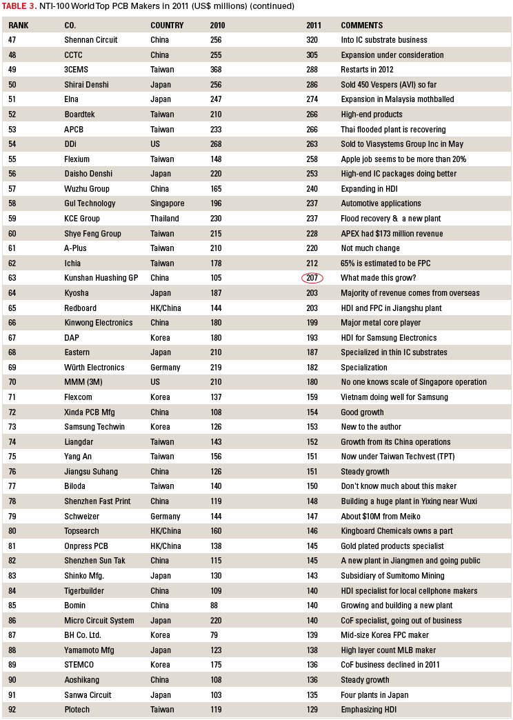
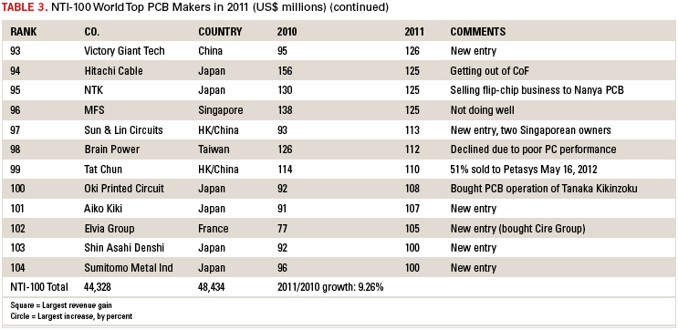
Table 3 lists the 2011 NTI-100. Although comments are included in the table, more extensive comments on certain fabricators are below.
Unimicron. Unimicron purchased Ruwel International of Germany and Clover Electronics of Japan in 2011 and took in partial revenues of these two into its fiscal 2011 revenue. The revenue in the table takes into consideration full-year accounts of Ruwel and Clover. Unimicron is rumored to be shutting one of its Shenzhen facilities (“Plato”). It plans to build new facilities in Jining in Shandong Province and Nantong along the Yangtze River, north of Shanghai. Its 2011 output in China jumped by 60%.
Nippon Mektron. Its subsidiary, Mektec Suzhou, obtained water permission for its long-awaited second plant, which is undergoing construction. It is scheduled to commence operations in the fourth quarter this year. Its Thai subsidiary, Mektec Thailand, flooded badly, but most of the equipment was moved to higher floors and saved. It could restart production as early as December, and become fully operational by March. The company is expected to reach $3 billion in revenue in fiscal 2012. Ibiden. Ibiden did poorly in flip-chip substrates for MPUs in 2011 due to sluggish PC shipments, but did very well with buildup MLBs for smartphones and tablets. It did well with IC substrates for baseband chips used for smartphones and tablets. It is reported that Ibiden is investing more than $2 billion to expand its overseas operations over the next three years, of which two-thirds will be used for PCB expansions. One-third of its fiscal 2011 revenue came from overseas production, but in fiscal 2013, Ibiden seeks to generate 60% of its revenue from overseas operations, particularly the Philippines and Malaysia. Its flip-chip substrate business is tops in the world, despite the slower 2011.
Zhen Ding. Zhen Ding is a business unit of Foxconn and was called Foxconn Advanced Technology prior to its Dec. 26, 2011, listing on the Taiwan Stock Exchange. A large portion of its revenue is said to come from FPC and FPC Assembly. The largest customer of its FPC business inclusive of FPC Assembly is said to be Apple Computer. It aims to become the largest PCB maker in the world in a few years, according to recent remarks by its CEO. It operates at two locations in Shenzhen, one at Yinkou, one at Qinghuangdao and one at Huai’an, all in China. Zhen Ding sold its Yantai facility to a business unit of Foxconn called Pan International prior to the stock listing because it was losing money, according to industry sources.
Tripod. Tripod’s revenue fell slightly in 2011 in terms of NT dollars due to poor PC demand. It has been reducing its dependency on the PC sector and diversifying its end-product markets. It is building new plants in Xiantao, about 100km west of Wuhan, along the Yangtze River. Two manufacturing buildings (of four planned) are nearly finished, and one will begin equipment installation toward the end of the third quarter and commence operations partially in the first quarter 2013. Automotive PCB is increasing at Tripod.
HannStar Board. HannStar Board completely absorbed GBM’s PCB units (GBM Yuanmao, CMK-GBM and GBM Chuangyi). GBM was building a facility in Chongqing. HannStar Board is trying to reduce its dependency on the notebook motherboard business. It made 93 million NB motherboards in 2011, mostly six and eight layers.
TTM Technologies. TTM is said to be strengthening its buildup MLB production capability both in technology and volume by adding a number of advanced laser drilling machines. Its US side of the business seems to be holding steady. Given the amount of investment in China, TTM’s future growth will come mainly from Chinese operations (TTM Asia Pacific, the former Meadville Technology).
Semco (Samsung Electro Mechanics Co). Semco benefited from high demand for Galaxy smartphones and tablets made by Samsung Electronics. However, 70% of its revenue came from IC substrates, flip-chip and wirebond types. Its Kunshan subsidiary, which makes buildup MLBs, also made a small contribution. In 2012, Semco is aiming at 1,900 billion won in revenue ($1.73 billion at 2011 exchange rates).
Nanya PCB. About $400 million of Nanya PCB’s revenue was derived from its Kunshan subsidiary, which has almost finished construction of a four-story PCB Plant 3 intended for wirebond IC substrates and for buildup MLBs. Nanya seems to be doing poorly in the first half of 2012, with a revenue decline of about 20% compared to the same period last year (parent only). Expected gains in the second half will hopefully compensate for a weak first half.
Young Poong Group. YP Group consists of Korea Circuits, Terranix, Interflex (FPC) and Young Poong Electronics (FPC). The combined FPC revenue of Interflex and Young Poong Electronics was $722 million, fourth largest in the world after Nippon Mektron, Sumitomo Denko Printed Circuits and M-Flex. Interflex’s gigantic eight-story building is completed in Ansan City, Korea, next to the head office of Korea Circuits. This plant will contribute greatly to the future revenue growth of YP Group. Buildup MLBs made by Korea Circuits are sold mainly to Samsung Electronics.
KB PCB Group. Kingboard Chemical’s PCB group consists of Elec & Eltek, Techwise, Evertek, Glory Faith, Top Faith and Express Circuits. Due to rising material costs and stiff price competition in the market, KB’s revenue was slightly below that of 2010. However, KB is in expansion mode, building huge plants for Elec & Eltek in Yangzhou (north of Nanjing), whose total production capability is planned to be 10 million sq. ft. per month when all five buildings are finished. Evertek in Kunshan is planning a four-story plant for buildup MLBs. Elec & Eltek Thailand was spared from the flooding last year. Top Faith seems to be building a new facility in Qingyuan, Guangdong Province.
Shinko Denki Industry. One of the major flip-chip package substrate makers (with Ibiden, Nanya PCB and SEMCO) for Intel chips, Shinko Denki, is building a major substrate plant in the city of Takaoka, Nagano Prefecture, for next-generation chips.
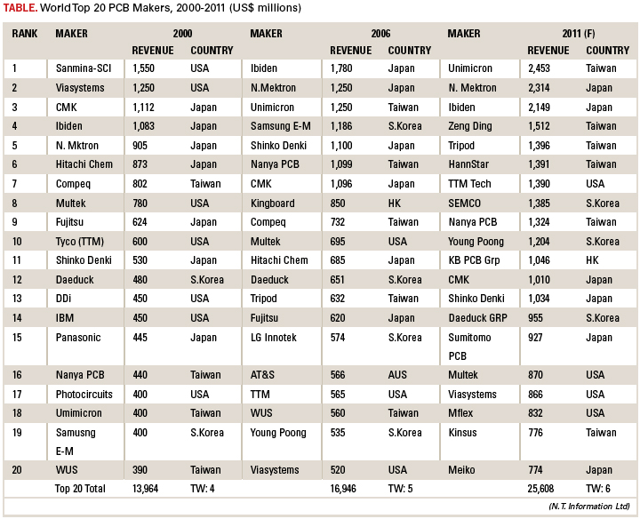
CMK. CMK’s revenue fell 10% in Japanese yen, but thanks to the rising yen, it remained in the NTI-$1B Club, which had 13 companies in 2011, up two from 2010. CMK was the largest automotive PCB maker in 2011, with revenue of $530 million, well ahead of No. 2 Viasystems. It expects that 60 to 65% of its revenue this year will come from automotive applications.
Daeduck Group. Daeduck Group consists of Daeduck Electronics and Daeduck GDS. Daeduck Electronics has two subsidiaries: APERIO, a maker of IC substrates, and Daeduck Electronics Philippines. GDS has a plant in Tianjing, which is rumored to be shut down. Its major customer is Samsung Electronics. Samsung is planning to ship 420 million cellphone units in 2012, of which 190 are to be Galaxy smartphones. Daeduck will benefit from this and is likely to join NTI-$1B Club in 2012.
Sumitomo Denko Printed Circuit. Several “Sumitomos” are engaged in the manufacture of PCBs: Sumitomo Mining (through a subsidiary, Shinko Mfg), Sumitomo Bakelite, Sumitomo Cable, Sumitomo Metal Electro Device and Sumitomo Denko. Sumitomo Denko has two FPC plants in Japan, two in China and one in Vietnam, about to be increased to two since it will be purchasing Sumitomo Bakelite’s Hanoi plant at the end of the third quarter. Forty-five to 50% of Sumitomo Denko’s revenue is said to come from sales to Apple.
Multek. Multek is a part of Flextronics and operates five plants in Zhuhai, China, one in Boeblingen, Germany, one in Sãn Paulo, Brazil, and one in Northfield, MN. Its FPC and rigid-flexible output seems to be increasing steadily, as is its high layer-count MLBs. Multek is a major buildup MLB maker in the world.
Viasystems Group. Some 48% ($412 million) of Viasystems’ bare board revenue came from automotive PCBs. It acquired DDi in May 2012, which will boost its military PCB output by several times. Its prorated revenue for bare PCBs in 2011 was $1.129 billion. Viasystems is one of the major high layer-count MLB manufacturers.
Multi-Fine Line Electronix. M-Flex sold its headquarters in Anaheim, CA, to DDi, which is now a Viasystems division, and moved to a new building in Irvine, CA. It used to have close to 400 employees in Anaheim, but is said to have only 50 now, with all other employees in China (Suzhou and Chengdu). Several years ago, over 80% of its revenue was from sales to Motorola. Now, more than 90% of its revenue comes from five major customers, including Apple and RIM.
Kinsus Technology. Kinsus Suzhou’s revenue contribution was next to nothing in 2011, but will be substantial in 2012, as its package substrate operations have been ramping since the beginning of 2012. Included in Kinsus’ revenue are sales from Piotek, formerly Boardtek, a subsidiary of Asustek. Kinsus PCB Group now belongs to Pegatron, a manufacturing arm of Asustek.
Meiko Electronics. Meiko sustained triple punches in 2011. The March earthquake/tsunami destroyed Meiko’s Ishinomaki plant, and the Fukushima plant was shut down for several months due to its proximity to the Fukushima nuclear plant, which exploded from the loss of its cooling pumps. Then, on Oct. 18, one of its two Wuhan plants was shut down for three months by Chinese authorities on suspicion of wastewater treatment violations, which was very much a political issue related to Apple’s suppliers (the “poison Apple” case, as the Chinese called it). The issue was resolved on Jan. 19, 2012. As a result, Meiko has been accelerating operation of its new Hanoi, Vietnam, plant. Despite all these problems, Meiko ended fiscal 2011 with a net profit. Meiko will see strong growth in 2012, with the Fukushima and Wuhan plants operational and the new Vietnam plant contributing greatly.
Compeq. Compeq has been doing well this year. It is one of the major PCB suppliers to Apple for all product lines (iPhones, iPods, iPads and iMac). Its Chongqing buildup MLB plant is scheduled to commence operation in the first quarter 2014.
Wus Group. Wus China was listed on the Shenzhen Stock Exchange in 2010. This China organization is separate from its Taiwan operation, but major ownership is common to both organizations. A new plant consisting of two buildings in Kunshan, about 20 minutes from the existing plant, is nearly completed, with total floor space of 2 million sq. ft. A second plant is in planning at Huangxi, 100 km east of Wuhan. Wus is one of the major high layer-count MLB makers in China. Of the $468 million revenue generated at Kunshan, well over $100 million came from MLBs above 18 layers.
AT&S. AT&S is Europe’s largest PCB maker, but the majority of its output came from its Shanghai plant ($403 million, or 56%). AT&S is also a major producer of automotive PCBs, with 2011 revenue of $120 million. It has been building a gigantic buildup MLB plant in Chongqing since July of 2011, and the building seems almost complete. It is scheduled to commence operation in early 2013. AT&S took a technical license from Panasonic to manufacture “ALIVH” products.
Fujikura. Fujikura is a major FPC manufacturer. Unfortunately, 95% of its output came from three plants in Thailand, two of which were completely flooded in fall 2011. One of the plants started partial operation in May, and the other is scheduled to restart operation in December, according to the company’s annual report. In the meantime, Fujikura purchased an FPC plant in Vietnam from bankrupted Sakai Denshi last December and commenced operation in January. At the same time, Fujikura selected land in Thailand high above sea level to build a new flex manufacturing plant, which is supposed to generate 30% of future revenue.
Gold Circuit Electronics. GCE is the second largest notebook motherboard maker, after HannStar Board. Unfortunately, its main notebook motherboard plant in Changzhu, China, had a fire and was disabled for some time. It has been restored.
Simmtech. Simmtech used to be Chungbuk Electronics. When it started to enter the single-in-line memory module business, it changed its name to Simmtech. In the last several years, Simmtech has been growing rapidly in the IC substrate market as well. It built a plant in Xian, China, to supply memory module circuits to Micron and Samsung Electronics.
Nitto Denko. Nitto Denko is a major Japanese FPC maker with plants in Japan, China (Suzhou) and Vietnam (near Ho Chi Minh City). It is building a new plant next to the existing plant in Vietnam.
Chin Poon Industrial. Chin Poon has several plants in Taiwan and a plant with two buildings in Changshu, China. It is the third largest automotive PCB maker in the world, with $300 million automotive revenue. Its Thailand subsidiary (minority share) was badly damaged by the flooding in the fall of 2011, but is fully restored.
Unitech Electronics. One of the largest buildup MLB makers in the world, Unitech built a new buildup plant in Ilan, Taiwan, which started operation in 2011. It has a provision to build a plant near Nanjing, but no concrete plan is set at this time, it seems. PID (Panasonic Industrial Devices). Formerly Panasonic Electronic Devices, and inventor and licensor of ALIVH technology, PID built a second ALIVH plant in Taiwan (Tayuan) and another ALIVH plant in Vietnam (Hanoi). Its overseas ALIVH production capability will triple when these two new plants become fully operational this year.
LG Innotek. It is said that LG Innotek supplies over 80% of its output to its parent, LG Electronics. Since LGE did poorly in cellphones in 2011, LG Innotek also did poorly. It decided to exit the high layer-count MLB business in 2010, which is a shame because it had very high technology in this field. The reason for the exit is that the market for high layer-count MLBs is rather small and is not growing compared to other fields such as IC substrates and buildup MLBs. So, now, LG Innotek concentrates on IC substrates and buildup MLBs. It supplies buildup MLBs (“any layer” type) for Apple’s smartphones.
Founder Technology. Owned by Beijing University, Founder Group went into the PCB business in 2004 when it purchased Zhuhai Multilayer. Since then, it acquired a quickturn and prototype maker in Hangzhou and built two new PCB plants: one in Zhuhai and the other in Chongqing. Zhuhai “Fushan Branch” plant in Doumen district of Zhuhai consists of four operations: buildup MLB, QTA and prototyping, R&D and IC substrate. The last operation is called ACCESS (Advanced Chip Career Electronic Substrate Solutions). ACCESS is a JV between Founder and Israeli substrate maker Amitek. (ACCESS’ revenue – $70 million in 2011 – is not included with Founder’s.) Founder built its second buildup MLB plant next to its existing site early this year and a separate quickturn plant at its Zhuhai Fushan Branch last year. Founder is one of what the author calls “three musketeers of China,” the others being CCTC and Shennan Circuits.
Shennan Circuits. A division of AVIC Group (Aviation Industry of China), which makes jet fighter airplanes, helicopters, automobiles, missiles and jet engines among other things, Shennan Circuits is one of the China’s best high layer-count MLB builders, with two plants in Shenzhen (Nanshan and Longgang districts). In 2011, it commenced production of BGA substrates and has been negotiating with Wuxi government to build a new BGA plant there.
China Circuit Technology Corp. CCTC is one of the large makers of buildup MLBs for local cellphone makers. CCTC has two plants in Shantou, Guangdong Province, a small plant in Shenzhen and another small one in Shichuwan Province. CCTC belongs to Go-World Group, which also has a laminate manufacturing subsidiary.
DDi. DDi, the second-largest PCB maker in North America after TTM, was purchased by Viasystems Group in May. This purchase boosts Viasystems’ military portion of its PCB business to well over $100 million.
Wuzhu Group, Shenzhen Fast Print, Shenzhen Sun Tak and Bomin Electronics. These three makers may be called second tier “four musketeers of China.” All have substantial expansions ongoing in various parts in China: Wuzhu in Dongguang, Fast Print in Yixing, Suntak in Jiangmen and Bomin in Meizhou.
Tat Chun Circuits. Some 51% of Tat Chun was acquired by Korean high layer-count MLB maker ISU Petasys in May of this year. “ISU” in Korean means “Pear Tree, or 梨樹. Peta is 10 to the 12th. The parent company, ISU Chemical, named it as Petasys to wish that it would grow to “infinity.” Tat Chun has had a business alliance with Japan’s Toppan-NEC, a competitor of ISU Petasys for Cisco’s programs. ISU Petasys is the largest supplier to Cisco. What is going to happen with Tat Chun, Toppan-NEC and ISU Petasys is beyond this author’s imagination. Good luck to all parties involved.
Ed.: For a larger version of Table 3, right-click on each table, then click View Image and increase the size.
If readers have questions about other NTI-100 entries, the author would be happy to respond.
One final comment: The “80-20” rule normally applies to the amount of market share controlled by 20% of the manufacturers in the same field. It is estimated that there are 2,600 to 2,800 PCB companies in the world today. The 104 companies on the NTI-100 list represent 3.7% of the total. The total revenue ($48 billion) of these 104 makers accounted for 81% of the world output ($59 billion). Therefore, in the PCB field, the rule may be more like “90-10”; that is, the big get bigger and faster.
Once a PCB manufacturer’s revenue reaches a certain level, say, $500 million per annum, it must keep running, meaning continuous investment. Some companies are taking a different path, specializing in a niche market with niche products. Which is better?
Printed circuit boards are a critical commodity. Here’s how to treat them as such.
Electronics quality and reliability are highly dependent on the capabilities of the manufacturer. Manufacturing issues are one of the top reasons companies fail to meet warranty expectations. These problems can result in severe financial pain and loss of market share. What a surprising number of engineers and managers fail to realize is that focusing on processes addresses only part of the issue. Supplier selection also plays a critical role in the success or failure of the final product.
Designing printed circuit boards today is more difficult than ever due to significantly increased density, higher lead-free process temperature requirements and associated changes required in manufacturing. Many changes have taken place throughout the entire supply chain regarding the use of hazardous materials and the requirements for recycling. The RoHS and REACH directives have caused many suppliers to the industry to change their materials and processes. Everyone designing or producing electronics has been affected.
PCBs should always be considered a critical commodity. Without stringent controls in place for PCB supplier selection, qualification and management, long-term product quality and reliability are neither achievable nor sustainable. Here, we discuss some best practices and recommendations for improving your PCB supply chain.
First, create a PCB commodity team with at least one representative each from design, manufacturing, purchasing and quality/reliability. The team needs to meet on a regular basis to discuss new products and technology requirements in the development pipeline. These meetings can take place through conference calls or via onsite visits. Pricing, delivery and quality performance issues with existing PCB suppliers should be reviewed. The team is also responsible for identifying new suppliers and creating supplier selection and monitoring criteria.
Second, establish initial PCB supplier selection criteria. The criteria should be unique to your business and products, but some general selection criteria include:
Time in business.
Revenue.
Growth.
Employee turnover.
Training program.
Certified to standards you require (IPC, MIL-Spec, ISO, etc.).
Capable of producing the technology you need as part of their mainstream capabilities.
Don’t build in process “niches” where suppliers claim capability, but little volume is built there.
Have quality and problem-solving methodologies in place.
Have a technology roadmap.
Have a continuous improvement program in place.
Ideally, the suppliers demonstrate long-term stability from both quality and business perspectives. Multiple factory locations and risk mitigation programs can further protect against catastrophic political and weather-related events. After this initial screening, visit the PCB suppliers that seem to be appropriate matches. Site visits to the actual fabrication facility by personnel knowledgeable in PCB fabrication techniques are crucial. The site visit is the best opportunity to review process controls, quality monitoring and analytical techniques, storage and handling practices and conformance to generally acceptable manufacturing practices. It is also the best way to meet and establish relationships with the people responsible for manufacturing your product.
After choosing some potential PCB suppliers, the true qualification work begins. Qualifying a PCB supplier is always a two-step process. The first step is to qualify both a design and the PCB manufacturer through rigorous product and test-vehicle-based evaluations. The PCBs built for qualification should be evaluated to the standards you require by both the PCB supplier and your company (or an independent lab). The second qualification step is to initiate ongoing testing to monitor outgoing quality through a combination of test vehicle and lot qualification.
How do you verify a PCB supplier is capable of meeting your reliability requirements? There are currently six common methods for testing and qualifying PCBs:
Modeling and simulation.
Cross-sectioning combined with solder float/shock tests.
Thermal shock testing (also
thermal cycling).
Printed Board Process Capability, Quality, and Relative
Reliability (PCQR2).
Interconnect stress testing (IST).
Highly Accelerated Thermal
Shock (HATS).
Very early in the design cycle, software simulation and modeling can be performed. As an example, DfR has implemented IPC-TR-579 into an automated design analysis software called Sherlock to permit rapid assessment of basic PCB robustness. IPC-TR-579 documents a “Round Robin Reliability Evaluation of Small Diameter (<20 mil) Plated Through Holes in PWBs.” This activity was initiated by IPC and published in 1988.
The objectives were to confirm sufficient reliability, benchmark different test procedures, evaluate influence of PTH design and plating, and develop a model. Some advantages of the IPC-TR-579 model are that it is analytical, validated through testing, and comments on the relative influence of design and material parameters. However, the validation data are over 18 years old. The model is unable to assess complex geometries, and it is difficult to assess the effect of multiple temperature cycles. The model also uses simplified assumptions (linear stress-strain above yield point). Finally, the model does not account for the effect of via fill and does not consider other failure modes such as knee cracking and wall-to-pad separation.
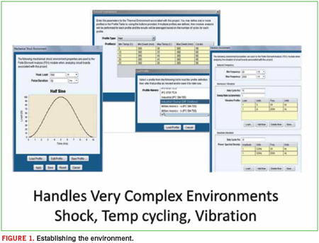
To successfully model a PCB design, the first step is to define the environment (Figure 1). Test, field or both environments can be modeled.
The second step is to upload the actual design information. Thermal maps can also be imported, if appropriate. The third step is to select the laminate and prepreg material. With this information, the stackup and copper percentage are automatically identified. Then, the PTH fatigue analysis can be performed.
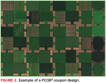
Another method is to qualify the design and manufacturer through the PCQR2 database and program. The program consists of a coupon design, a test standard, and a database of participating suppliers. The coupon has an 18" x 24" layout with 352 1" x 1" test modules (Figure 2). It can consist of two to 24 layers (rigid, rigid-flex) and requires builds of three panels and three non-consecutive lots with six times simulated assembly and HATS cycling.
An advantage of the PCQR2 program is that it is available in an industry standard (IPC-9151) format. It is easy to follow and provides real data for understanding PCB supplier capabilities (Table 1). It also provides a comparison to the rest of the industry through the use of an anonymous database. However, it is an IPC-approved monopoly and can be expensive, ranging from $2,000 to $5,000, not including panel costs, per supplier and facility evaluated.
Interconnect stress testing (IST) is the overwhelming favorite of high-reliability organizations for lot-based qualification testing. IST uses small (1" x 4") coupons that can fit along the edge of a product panel. Testing is automated, widely used and has the ability to drive barrel fatigue and post-separation failures. The large number of holes (up to 300) and continuous resistance monitoring make it far superior to cross-sectioning. And, in most cases, IST is a more cost-effective option. There are some potential issues to be aware of, however. The IST coupon design is critical. Preconditioning, test frequency, maximum temperature and failure requirements must all be specified. Test frequency can range from every lot to every month to every quarter. Maximum temperatures of 130˚, 150˚, and 175˚C are most commonly used. And, different markets and organizations specify different times to failure, with 300, 500, and 1000 cycles most common.
Next, if your product line ranges from simple to highly complex, consider tiering (low, middle, high) suppliers. Tiering permits strategic supplier selection to maximize cost savings and quality against your product design requirements. Match supplier qualifications to the complexity of the product. Some criteria for tiering suppliers include:
Finest line width.
Finest conductor spacing.
Smallest drilled hole and via.
Impedance control.
Specialty laminates or construction needed (PTFE, flex, mixed technologies).
Buried resistance or capacitance.
Use of HDI, microvias, blind or buried vias.
Minimize use of suppliers that outsource critical areas of construction. Again, do not exist in the margins of any supplier’s process capabilities.
Relationship management is another important element of success. Ideally, you are a partner with your PCB suppliers. This is especially critical if you have low volumes, low spend, or high technology and reliability requirements. Good partnering practices include:
Routine conference calls between your PCB commodity team and each PCB supplier’s equivalent team.
Quarterly business reviews (QBR) that review spend, quality, and performance metrics, and also include “state of the business updates.” Business updates can address any impending changes, such as factory expansion, move, or relocation, critical staffing changes, new equipment/capability installation, etc. The sharing is done from both sides. You also share any data that would help strengthen the business relationship: business growth, new product and quoting opportunities, etc. At least once per year, the QBRs should be site meetings that alternate between your site and the supplier factory. The factory supplier site visit can double as the annual onsite visit and audit that you should be performing.
Ongoing supplier “lunch and learns” or technical presentations held at your facility or via webinar. Suppliers routinely provide education regarding their processes and capabilities. They can educate your technical community on PCB design for manufacturing, quality, reliability and cost factors. They can also inform you on pitfalls, defects, and newly available technology. This activity is usually performed free of charge, and suppliers may even provide free lunch to encourage attendance. It also gives you an opportunity to educate them on your needs.
Supplier scorecards should exist and be used on a rolling quarterly and yearly basis. Typical scorecards include both objective and subjective metrics. Objective metrics include on-time delivery, cost, PPM defect rates, and quality excursions, which require root cause corrective actions. Subjective measures include communication issues (speed, accuracy, responsiveness to quotes) and cost-savings suggestions. And, there should be detailed discussion of any recalls, notifications or scrap events exceeding a certain threshold.
Finally, make sure that any supplier has a robust continual quality improvement program in place. At a minimum, consider monitoring and reviewing the top three PCB factory defects, process control and improvement plans for those top defects, yield and scrap reporting for your products and feedback on general issues facing the PCB industry.
The foundation of a reliable product is a reliable PCB. Having a comprehensive strategy for selecting and qualifying PCB suppliers ensures the foundation is strong.
Cheryl Tulkoff is senior member of the technical staff and Craig Hillman, Ph.D., is CEO and managing partner of DFR Solutions (dfrsolutions.com); This email address is being protected from spambots. You need JavaScript enabled to view it.. DFR will be exhibiting in September at PCB West 2012 at the Santa Clara (CA) Convention Center.
The Japanese Ministry of Economy, Trade and Industry (METI) released June’s production data for the electronics industry in Japan last week. Now that a snapshot for the first half is available, we can review a few market trends and assess our plans for the remainder of the year.
Some 20 months after Altium’s announcement it would move its suite of PCB tools to the cloud, a handful of PCB industry veterans are vying to be the first to offer pre-CAM analysis through that same new channel.
Under the name Iron Atom, Iain Wilson and Alessandro Federici are in the last cycle of beta testing this new model, making proprietary CAM software available for individual, one-off use, without the need for a license or maintenance agreement.
The tool, in this case, is Ucamco’s Integr8tor front-end engineering software. Designers and CAM engineers can now access the software via Iron Atom’s website, choosing the features to run and preferred CAM output (UCAM, Gerber 274X or ODB++).
Using the cloud – really, a group of servers that reside with a third party instead of with the user – is essentially a different medium for tool rental. But the model will allow lighter users the opportunity to take advantage of the Ucamco’s stackup, registration and design rule checks without the cost and hassle of purchasing and installing a full license.
Users create a job, upload their files, and configure which outputs they desire. Reports are generated in minutes, Iron Atom says. Recognizing IP control is a concern, Iron Atom opted for a proven commercial technology partner. The site runs on Amazon’s EC2 cloud computing platform, and secure jobs can be run on Amazon’s GovCloud, which is approved for US ITAR products. “There are multiple levels of security, says Federici. “Design files never make it to the Iron Atom website. They all go straight to Amazon.”
“All processing is done in an instant,” adds Wilson, “with results going back to the user.” Results include a PDF report with design analysis and XML data files. CAM ready data and layer images are optional. Jobs are then deleted from the server as a security measure.
Support is supplied by Iron Atom, but according to Wilson, the need is minimal. “We’ve found Integr8tr provides 80% to 90% of the data automatically. And we report back to the user if problems are found.” Custom design rule checks and manual processing are also options.
To do all this, Iron Atom runs a full feature version of Integr8tor 7.1, Ucamco’s latest release. Iron Atom charges an undisclosed fee per use, with Ucamco getting a percentage of every transaction. (A small surcharge is applied for extra outputs.)
The concept is undergoing its second round of beta testing, having been tested by a number of North American and European fabricators, plus a couple more in China, that have been Ucamco customers. Iron Atom is seeking additional beta partners; Wilson can be reached at This email address is being protected from spambots. You need JavaScript enabled to view it.. “We have maybe one more month of beta before we get fully online,” he told PCD&F.
Wilson, who has been a CAM engineer since 1996, says the inspiration for Iron Atom was a “light bulb moment.”
“It’s nice to be the first to offer this. It’s difficult task for CAD vendors because of the type of processing involved. I think it’s a difficult step. But I’m pretty confident that in 10 years’ time, we will say, ‘Remember when we used to have to buy servers.’”
While Iron Atom can scale for larger users, initial interest most likely would come from lighter users. However, Wilson says, “We could see bigger shops using it if they have a spike in demand. Even if they have an in-house solution, it takes up time and resources in their CAM machines.”
For the user, the experience poses the advantages of access to DfM checks and analysis with no installation time or setup or maintenance costs. “My experience with Ucamco has always been very good,” Wilson says. “The level of automation is exceptionally high. The end-user wants to get their DfM done; they don’t want to use additional software.”
The deal between Ucamco and Iron Atom is nonexclusive. For its part, Ucamco sees Iron Atom as an additional pipeline to reach small- to medium-sized customers who otherwise might not be prospects.
Mike Buetow is editor in chief of PCD&F (pcdandf.com); This email address is being protected from spambots. You need JavaScript enabled to view it..
Results of a two-year study of various electroless nickel baths.
Many Pb-free alloy formulations, including SAC alloy (consisting of 3-4% silver, 0.5-1% copper and the balance tin), have been developed to replace leaded solder (typically, SnPb), and used successfully to manufacture and assemble printed circuit boards. As Pb-free solder can leave bumps on the traces during HASL (hot air solder leveling), many alternate surface finish processes have been investigated to overcome this challenge.
Alternate surface finishes for Pb-free solder have been developed and used for leadless components with pitches of 4 mils (0.01mm) or less, on which BGAs, TSOPs, etc. are mounted and soldered. These alternate surface finishes include:
Several formulations of ENIG plating have been tried. Here, we discuss a successful formulation of ENIG that has been in continuous use in large-scale PCB production for more than two years.
Formulations of electroless nickel on copper. The following Bath I showed good results for electroless nickel plating on copper pads and PTH holes.
Bath I: Nickel chloride (Nicl2.6H2O): 20g per liter. Sodium hypophosphite (NaH2PO2.H2O): 15g per liter. Acetic acid (CH3COOH): 20ml per liter. DL-Malic acid, CH2 (COOH).CH (OH).COOH: 20g per liter. Glycine (NH2CH2COOH): 5g per liter. Boric acid (H3BO3): 2g per liter. pH – 6.5 to 6.7 (adjusted with NaOH and HCl) Temperature: 70o to 72oC. Time to get 5 to 6µm of eNickel on copper: 25 to 30 min.
Process sequence. The process sequence was as follows: 1) acid cleaner, 2) swill, 3) micro-etch, 4) swill thoroughly, 5) pre-activator, 6) activator, 7) swill, 8) post-activator, 9) swill thoroughly, 10) electroless nickel plating, 11) swill, 12) immersion gold plating, 13) swill, 14) hot water dip, 15) dry.
This bath was further studied thoroughly by varying the various ingredient chemical compositions. Graphs were plotted to show the optimum condition to get the best and fastest results of deposition of electroless nickel deposit on copper. Each time, a single chemical ingredient (out of six chemicals) was varied and studied at temperatures of 70˚, 75˚ and 80˚C.
Cleaned, pre-weighed 1" x 1" copper specimens were used throughout the experiment, and the nickel deposit thickness obtained and calculated by the weight gain method. This was cross-checked using an x-ray fluorescence thickness tester, and the results were within ±5% difference.
Figures 1 to 11 show the thickness results as obtained by weight-gain method, demonstrating the optimum condition of the bath chemical composition.
Table 1 shows the optimum results.
Optimum composition of eNi bath (Bath II): Nickel chloride (Nicl2.6H2O): 15g per liter. Sodium hypophosphite (NaH2PO2H20): 14g per liter. Acetic acid (CH3COOH): 22ml per liter. DL-Malic acid, CH2 (COOH). CH (OH). COOH: 18g per liter. Glycine (NH2CH2COOH): 7g per liter. Boric acid (H3BO3): 2g per liter. pH: 6.8 to 6.9 (adjusted with NaOH and HCl). Temperature: 70o to 72oC. Thickness: 6.74 to 9.0µm of Ni in 30 min. Time: 30 to 35 min. Final (optimum) composition of eNi bath: Nickel chloride, Nicl2.6H2O: 15g per liter. Sodium hypophosphite, NaH2PO2H20: 14g per liter. Acetic acid (CH3COOH): 22ml per liter. DL-Malic acid, CH2 (COOH). CH (OH). COOH: 18g per liter. Glycine (NH2CH2COOH ): 7g per liter. Boric acid (H3BO3): 2g per liter. pH: 6.8 to 6.9 (adjusted with NaOH and HCl). Temperature: 80o to 82oC to get 9.44µm of nickel. Time: 25 to 30 min.
This bath was prepared and used for 12 months to verify and establish the results. It was consistent in providing a thickness of 8-9µm of nickel at 80oC in 25-30 min.
Composition of nickel deposit. The deposited nickel was subjected to EDAX analysis to reveal the composition. Results are shown in Figures 13 and 14. The deposit contains 12.23 to 13.74% of phosphorus.
Formulation of immersion gold on nickel: Gold potassium cyanide K Au (CN)2: 3g per liter. Sodium hypophosphite: (NaH2PO2.H2O): 10g per liter. Sodium citrate: 50g per liter. Ammonium chloride (NH4 cl): 5g per liter. Temperature: 90±2oC. pH: 6.9 to 7.0. Time to get 0.03 to 0.05µm of gold on nickel: 15 to 20 min.
The thickness of gold was measured using an x-ray fluorescence tester. With these two formulations, standard deposits of electroless nickel gold were obtained for large-scale production.
Before shutting down, add 100ml of glycine solution (1gm per liter of glycine stock solution) to the working electroless nickel bath to avoid the possible deposition of nickel on the walls of the process vessel. With this precaution, the bath can easily be maintained for more than 100 days.
Before the start of the bath, analyze the nickel content and add required nickel chloride solution, sodium hypophosphite solution, adjust pH and start the dummy to plate.
This formulation has been found useful for volume production of ENIG plating.
References
Arthur K. Graham, ed., Electroplating Engineering Handbook, second edition, 1962. Kenneth E. Langford, Analysis of Electroplating and Related Solutions, 4th edition, Teddington, Draper, 1971.
Dr. T.S. Krishna Ram is chief executive (Techno-Commercial) at M/s. Meena Circuits Pvt. Ltd.; This email address is being protected from spambots. You need JavaScript enabled to view it..